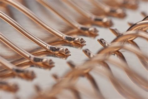
Introduction to Wire Bonding
Wire bonding is a critical process in the assembly of semiconductor packages, providing electrical connections between the integrated circuit (IC) and the package substrate or leadframe. This technology has been widely used for decades due to its affordability, flexibility, and reliability. Wire bonding involves attaching thin metallic wires, typically made of gold, aluminum, or copper, from the bond pads on the IC to the corresponding pads on the package substrate or leadframe.
Advantages of Wire Bonding
Wire bonding offers several advantages that make it a popular choice for semiconductor packaging:
- Cost-effectiveness: Wire bonding is an economical interconnection method compared to other technologies like flip-chip bonding or through-silicon vias (TSVs).
- Flexibility: Wire bonding allows for the connection of ICs with varying sizes and pad layouts, making it adaptable to different package designs.
- Reliability: When properly implemented, wire bonding provides reliable electrical connections that can withstand mechanical stress and environmental factors.
- Maturity: Wire bonding has been used for decades, and the technology has been continuously improved and optimized over time.
Wire Bonding Process
The wire bonding process involves several key steps to ensure reliable and high-quality interconnections.
1. Die Attachment
Before wire bonding can begin, the IC die must be securely attached to the package substrate or leadframe. This is typically done using die attach adhesives, such as epoxy or solder, which provide mechanical stability and thermal dissipation.
2. Wire Bonding
Once the die is attached, the wire bonding process can commence. There are two primary wire bonding techniques:
a. Ball Bonding
Ball bonding is the most common wire bonding method, primarily used with gold wire. The process involves the following steps:
- A gold wire is fed through a capillary tool, and a high-voltage electric discharge forms a gold ball at the end of the wire.
- The capillary tool presses the gold ball onto the bond pad of the IC, using a combination of heat, pressure, and ultrasonic energy to create a metallurgical bond.
- The capillary tool then moves to the corresponding pad on the package substrate or leadframe, forming a loop in the wire.
- The wire is then bonded to the substrate or leadframe pad using a similar combination of heat, pressure, and ultrasonic energy.
- Finally, the wire is cut, and the process is repeated for the next connection.
b. Wedge Bonding
Wedge bonding is typically used with aluminum or copper wire and is less common than ball bonding. The process involves the following steps:
- The wire is fed through a wedge-shaped tool.
- The wedge tool presses the wire onto the bond pad of the IC, using a combination of pressure and ultrasonic energy to create a bond.
- The tool then moves to the corresponding pad on the package substrate or leadframe, forming a loop in the wire.
- The wire is then bonded to the substrate or leadframe pad using a similar combination of pressure and ultrasonic energy.
- Finally, the wire is cut, and the process is repeated for the next connection.
3. Inspection and Testing
After wire bonding, the packages undergo visual inspection and electrical testing to ensure the quality and reliability of the interconnections. Visual inspection checks for wire bonding defects such as missing or misaligned bonds, while electrical testing verifies the continuity and performance of the connections.

Wire Bonding Materials
The choice of wire material depends on various factors, including cost, performance requirements, and compatibility with the bond pad metallization. The most common wire materials used in wire bonding are:
1. Gold Wire
Gold wire is the most widely used material for wire bonding due to its excellent electrical conductivity, corrosion resistance, and ease of bonding. Gold wire is typically used in ball bonding applications and is available in various diameters, ranging from 15 µm to 50 µm.
2. Aluminum Wire
Aluminum wire is an alternative to gold wire, offering cost advantages and compatibility with aluminum bond pads. However, aluminum wire is more prone to oxidation and requires a more controlled bonding process compared to gold wire. Aluminum wire is typically used in wedge bonding applications.
3. Copper Wire
Copper wire has gained popularity in recent years due to its lower cost compared to gold wire and better electrical and thermal conductivity. However, copper wire is more prone to oxidation and requires a more stringent bonding process control. Copper wire can be used in both ball and wedge bonding applications.

Wire Bonding Challenges and Advancements
As semiconductor devices continue to shrink in size and increase in complexity, wire bonding faces several challenges and opportunities for improvement.
1. Fine Pitch Bonding
With the increasing density of bond pads on ICs, the pitch (distance) between adjacent pads has decreased, requiring finer wire diameters and more precise bonding processes. Advanced wire bonders with high-resolution pattern recognition systems and improved bonding control have been developed to address this challenge.
2. Copper Wire Bonding
While copper wire offers cost and performance advantages, its susceptibility to oxidation and the need for a more controlled bonding process have limited its adoption. Recent advancements in copper wire bonding, such as the development of protective coatings and optimized bonding parameters, have helped overcome these challenges.
3. Multi-Tier Wire Bonding
As package designs become more complex, multi-tier wire bonding has emerged as a solution to increase interconnection density. In multi-tier wire bonding, wires are bonded at different heights, allowing for more connections within the same package area. This requires precise control of wire loop heights and advanced wire bonder capabilities.

Wire Bonding Applications
Wire bonding finds applications in a wide range of semiconductor packages and end-use markets.
1. Plastic Encapsulated Packages
Wire bonding is extensively used in plastic encapsulated packages, such as quad flat packages (QFPs), thin small outline packages (TSOPs), and ball grid arrays (BGAs). These packages are commonly used in consumer electronics, automotive, and industrial applications.
2. Hermetic Packages
Wire bonding is also used in hermetic packages, where the IC is sealed in a ceramic or metal package to provide enhanced protection against environmental factors. Hermetic packages are often used in aerospace, defense, and medical applications.
3. Power Semiconductor Packages
Wire bonding is used in power semiconductor packages, such as power QFPs and power modules, to provide high-current connections between the power devices and the package terminals. These packages are used in power management, motor control, and renewable energy applications.
Future Trends in Wire Bonding
As semiconductor packaging continues to evolve, wire bonding technology is expected to adapt and improve to meet new challenges.
1. Advanced Materials
Research is ongoing to develop new wire materials that offer better performance, reliability, and cost-effectiveness. For example, palladium-coated copper wire has been proposed as an alternative to gold wire, offering improved oxidation resistance and compatibility with a wider range of bond pad metallizations.
2. Automation and Industry 4.0
The integration of automation, machine learning, and data analytics in wire bonding processes is expected to increase in the future. This will enable real-time process monitoring, predictive maintenance, and optimization of bonding parameters, leading to improved yield and productivity.
3. Hybrid Bonding
The combination of wire bonding with other interconnection technologies, such as flip-chip bonding or TSVs, is expected to gain traction in the future. Hybrid bonding allows for the optimization of package performance, cost, and form factor by leveraging the strengths of different interconnection methods.
Conclusion
Wire bonding remains a critical and widely used interconnection technology in semiconductor packaging. Its affordability, flexibility, and reliability have made it the go-to choice for a wide range of applications. As semiconductor devices continue to advance, wire bonding technology is expected to evolve, with improvements in materials, processes, and automation. By understanding the fundamentals of wire bonding and staying informed about the latest advancements, semiconductor professionals can effectively leverage this essential technology in their package designs.
Frequently Asked Questions (FAQ)
1. What is the difference between ball bonding and wedge bonding?
Ball bonding uses a gold wire and involves the formation of a gold ball at the end of the wire, which is then bonded to the IC bond pad. Wedge bonding, on the other hand, uses aluminum or copper wire and involves directly bonding the wire to the bond pad using a wedge-shaped tool.
2. What factors influence the choice of wire material for wire bonding?
The choice of wire material depends on several factors, including cost, performance requirements, and compatibility with the bond pad metallization. Gold wire is the most common choice due to its excellent electrical conductivity and ease of bonding, while aluminum and copper wires offer cost advantages but require more controlled bonding processes.
3. How does wire bonding compare to other interconnection technologies like flip-chip bonding?
Wire bonding is generally more cost-effective and flexible compared to flip-chip bonding, as it can accommodate a wider range of IC sizes and pad layouts. However, flip-chip bonding offers higher interconnection density and better electrical performance, making it suitable for high-performance applications.
4. What are the key challenges in fine pitch wire bonding?
Fine pitch wire bonding requires the use of finer wire diameters and more precise bonding processes to accommodate the reduced distance between adjacent bond pads. This necessitates advanced wire bonders with high-resolution pattern recognition systems and improved bonding control to ensure reliable and high-quality interconnections.
5. How can automation and Industry 4.0 technologies benefit wire bonding processes?
The integration of automation, machine learning, and data analytics in wire bonding processes can enable real-time process monitoring, predictive maintenance, and optimization of bonding parameters. This can lead to improved yield, productivity, and quality control in wire bonding operations, ultimately reducing costs and enhancing the overall efficiency of semiconductor packaging processes.
| Wire Material | Advantages | Disadvantages |
|---|---|---|
| Gold | – Excellent electrical conductivity – Corrosion resistance – Ease of bonding |
– Higher cost compared to other materials |
| Aluminum | – Lower cost compared to gold – Compatibility with aluminum bond pads |
– Prone to oxidation – Requires more controlled bonding process |
| Copper | – Lower cost compared to gold – Better electrical and thermal conductivity |
– Prone to oxidation – Requires stringent bonding process control |
No responses yet