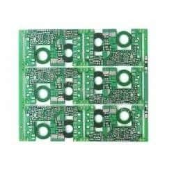
Introduction to PCB-PTH Technology
Printed Circuit Board (PCB) design has evolved significantly over the years, with various technologies being developed to enhance the functionality, reliability, and durability of electronic devices. One such technology is Plated Through Hole (PTH), which has become a crucial component in modern PCB design. In this article, we will explore the reasons why PCB-PTH technology is widely used and the benefits it offers in electronic device manufacturing.
What is PCB-PTH Technology?
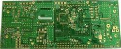
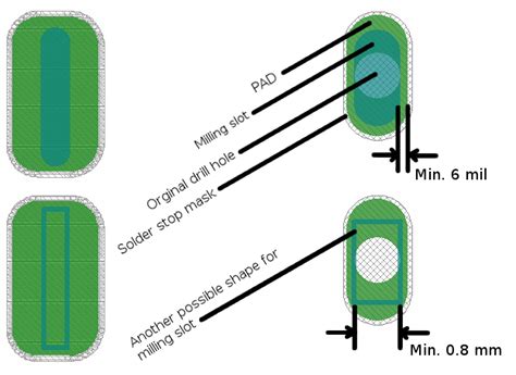
PCB-PTH technology involves creating a hole in the PCB board and then plating the inside of the hole with a conductive material, typically copper. This process creates a reliable electrical connection between the layers of the PCB, allowing for the passage of electrical signals and current. PTH technology is used in both single-sided and double-sided PCBs, as well as in multi-layer boards.
Advantages of PCB-PTH Technology
- Enhanced Mechanical Strength
- Improved Electrical Connectivity
- Better Heat Dissipation
- Increased Reliability
- Compatibility with Through-Hole Components
Enhanced Mechanical Strength
One of the primary reasons for using PCB-PTH technology is the enhanced mechanical strength it provides to the PCB. The plated holes act as anchors, holding the layers of the PCB together and preventing delamination. This is particularly important in applications where the PCB is subject to vibration, shock, or physical stress.
Comparing PTH and Non-PTH PCBs
| Parameter | PTH PCBs | Non-PTH PCBs |
|---|---|---|
| Mechanical Strength | High | Low |
| Delamination Resistance | High | Low |
| Vibration Resistance | High | Low |
| Shock Resistance | High | Low |
As evident from the table above, PTH PCBs excel in terms of mechanical strength compared to their non-PTH counterparts. This makes them ideal for use in demanding applications such as automotive, aerospace, and military electronics.
Improved Electrical Connectivity
Another significant benefit of PCB-PTH technology is the improved electrical connectivity it offers. The plated holes create a low-resistance path for electrical signals to travel between layers of the PCB, ensuring reliable and efficient signal transmission.
Signal Integrity in PTH PCBs
PTH technology helps maintain signal integrity by reducing the risk of signal loss or distortion. The plated holes provide a controlled impedance environment, which is crucial for high-speed digital signals. Additionally, PTH vias can be strategically placed to minimize crosstalk and electromagnetic interference (EMI).
Comparing Signal Integrity in PTH and Non-PTH PCBs
| Parameter | PTH PCBs | Non-PTH PCBs |
|---|---|---|
| Signal Loss | Low | High |
| Signal Distortion | Low | High |
| Crosstalk | Low | High |
| EMI Susceptibility | Low | High |
The table above highlights the superior signal integrity characteristics of PTH PCBs compared to non-PTH PCBs. This makes PTH technology essential for applications that require high-speed, low-loss signal transmission, such as telecommunications, networking, and high-performance computing.

Better Heat Dissipation
PCB-PTH technology also offers better heat dissipation compared to non-PTH designs. The plated holes act as thermal vias, providing a path for heat to dissipate from the components on the PCB to the other layers and eventually to the environment.
Thermal Management in PTH PCBs
Effective thermal management is crucial for ensuring the long-term reliability and performance of electronic devices. PTH technology helps in this regard by:
- Distributing heat evenly across the PCB
- Reducing hotspots around high-power components
- Enabling the use of heat sinks and other thermal management solutions
Comparing Thermal Performance of PTH and Non-PTH PCBs
| Parameter | PTH PCBs | Non-PTH PCBs |
|---|---|---|
| Heat Distribution | Even | Uneven |
| Hotspot Formation | Low | High |
| Thermal Management Options | More | Limited |
As shown in the table above, PTH PCBs offer better thermal performance than non-PTH PCBs. This makes them suitable for applications that generate significant amounts of heat, such as power electronics, LED lighting, and high-performance computing.
Increased Reliability
PCB-PTH technology contributes to the overall reliability of electronic devices by providing a robust and stable platform for components. The enhanced mechanical strength, improved electrical connectivity, and better heat dissipation offered by PTH PCBs all contribute to increased reliability.
Factors Affecting PCB reliability
Several factors can impact the reliability of a PCB, including:
- Environmental conditions (temperature, humidity, vibration, etc.)
- Manufacturing quality
- Component selection and placement
- PCB design and layout
PTH technology helps address these factors by providing a solid foundation for the PCB and its components. The plated holes ensure a reliable connection between layers, while also offering protection against environmental stresses.
Comparing Reliability of PTH and Non-PTH PCBs
| Parameter | PTH PCBs | Non-PTH PCBs |
|---|---|---|
| Environmental Resistance | High | Low |
| Manufacturing Defect Tolerance | High | Low |
| Component Stability | High | Low |
| Long-term Reliability | High | Low |
The table above demonstrates the superior reliability characteristics of PTH PCBs compared to non-PTH PCBs. This makes PTH technology the preferred choice for applications that require high reliability, such as medical devices, industrial control systems, and aerospace electronics.
Compatibility with Through-Hole Components
PCB-PTH technology is essential for accommodating through-hole components, which are still widely used in many electronic devices. Through-hole components, such as connectors, transformers, and large capacitors, require a mechanical anchor to the PCB, which is provided by the plated holes.
Advantages of Through-Hole Components
Despite the increasing popularity of surface-mount components, through-hole components still offer several advantages, including:
- Ease of manual assembly and repair
- Higher power handling capability
- Better mechanical stability
- Lower cost for certain component types
Combining PTH and SMT Technologies
Many modern PCBs employ a combination of PTH and Surface Mount Technology (SMT) to leverage the benefits of both technologies. PTH is used for through-hole components and to provide mechanical strength, while SMT is used for smaller, more densely packed components. This hybrid approach allows for the creation of compact, high-performance electronic devices.
FAQ
-
Q: Can PTH technology be used in multi-layer PCBs?
A: Yes, PTH technology is commonly used in multi-layer PCBs to establish electrical connections between the layers and to provide mechanical strength. -
Q: Is PTH technology suitable for high-frequency applications?
A: While PTH technology can be used in high-frequency applications, it may not be the optimal choice. For high-frequency signals, controlled impedance designs and specialized via structures, such as blind and buried vias, are often preferred. -
Q: How does PTH technology compare to press-fit technology?
A: PTH and press-fit technologies serve similar purposes but have some differences. PTH involves plating the holes with a conductive material, while press-fit relies on the mechanical compression of a component lead against the hole wall. Press-fit technology is often used for high-reliability applications, such as automotive and aerospace electronics. -
Q: Can PTH technology be used with flexible PCBs?
A: Yes, PTH technology can be used with flexible PCBs, although the design and manufacturing process may be more challenging due to the nature of the flexible substrate. Special considerations, such as hole size, plating thickness, and component selection, must be taken into account. -
Q: What are the limitations of PTH technology?
A: Some limitations of PTH technology include the need for larger hole sizes compared to modern SMT components, which can limit the routing space on the PCB. Additionally, the drilling and plating processes used in PTH can be more time-consuming and costly compared to SMT-only designs.
Conclusion
PCB-PTH technology is a crucial component in modern electronic device design, offering numerous benefits such as enhanced mechanical strength, improved electrical connectivity, better heat dissipation, increased reliability, and compatibility with through-hole components. By understanding the advantages of PTH technology and its applications, PCB designers and engineers can create more robust, reliable, and high-performance electronic devices.
As the electronics industry continues to evolve, PCB-PTH technology will likely remain an essential tool in the designer’s arsenal, enabling the creation of innovative and dependable products across a wide range of industries and applications.
No responses yet