Understanding BGA Packages and Fanout
BGA packages are surface-mount devices that utilize an array of solder balls underneath the component to establish electrical connections with the PCB. These packages offer several advantages, including:
- High pin count density
- Reduced package size
- Improved thermal and electrical performance
However, routing traces from the BGA pads to other components on the PCB can be challenging due to the high density of connections. This is where fanout strategies come into play.
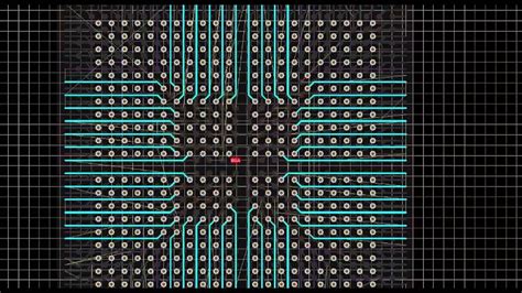
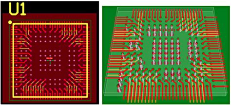
Fanout refers to the process of routing traces from the BGA pads to other layers of the PCB, allowing for the connection of the BGA to other components. There are several fanout strategies to consider, each with its own advantages and disadvantages.
Types of BGA Pad Configurations
Before diving into fanout strategies, it’s essential to understand the different types of BGA pad configurations. The two primary configurations are:
- Non-Solder Mask Defined (NSMD) Pads:
- The solder mask opening is larger than the copper pad size
- Allows for better solder joint formation and self-alignment during reflow
-
Provides higher tolerance for pad-to-mask misalignment
-
Solder Mask Defined (SMD) Pads:
- The solder mask opening is smaller than the copper pad size
- Offers better control over the solder joint size and shape
- Provides higher copper packing density
The choice between NSMD and SMD pads depends on factors such as the BGA package type, PCB manufacturing capabilities, and design requirements.

BGA Fanout Strategies
There are several fanout strategies to consider when designing a PCB with BGA components. Each strategy has its own merits and limitations, and the choice depends on the specific design constraints and requirements.
1. Via-in-Pad (VIP) Fanout
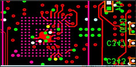
Via-in-Pad (VIP) fanout involves placing vias directly within the BGA pads, allowing for direct connection to the inner layers of the PCB. This strategy offers several advantages:
- Reduces the need for additional routing layers
- Minimizes the overall PCB size
- Improves signal integrity by reducing trace lengths
However, VIP fanout also has some limitations:
- Requires precise via placement and drilling
- May lead to solder wicking into the vias during reflow
- Increases the complexity of PCB assembly and inspection
To mitigate solder wicking issues, various techniques can be employed, such as using filled or capped vias, or applying a solder mask plug over the via.
2. Dog-Bone Fanout
Dog-bone fanout, also known as teardrop fanout, involves placing a teardrop-shaped pad adjacent to the BGA pad and connecting them with a short trace. The fanout trace then extends from the teardrop pad to the inner layers of the PCB. This strategy offers several benefits:
- Allows for easier routing and trace escape
- Reduces the risk of solder wicking compared to VIP fanout
- Provides better visual inspection capabilities
However, dog-bone fanout also has some drawbacks:
- Increases the overall PCB size due to additional pad space
- May require additional routing layers
- Can lead to signal integrity issues if not properly designed
To optimize dog-bone fanout, designers should consider factors such as pad size, trace width, and spacing between adjacent teardrops.
3. Through-Via Fanout
Through-via fanout involves placing vias adjacent to the BGA pads and connecting them with short traces. The fanout traces then extend from the vias to the inner layers of the PCB. This strategy provides several advantages:
- Allows for easier routing and trace escape compared to VIP fanout
- Reduces the risk of solder wicking
- Offers better thermal dissipation compared to dog-bone fanout
However, through-via fanout also has some limitations:
- Increases the overall PCB size due to additional via space
- May require additional routing layers
- Can lead to signal integrity issues if not properly designed
To optimize through-via fanout, designers should consider factors such as via size, via-to-pad spacing, and the number of vias per BGA pad.

Fanout Layer Considerations
When designing the fanout for a BGA component, it’s crucial to consider the number and arrangement of layers used for fanout. The choice of fanout layers depends on factors such as the BGA package size, pin count, and routing density.
1. Single-Layer Fanout
Single-layer fanout involves routing all the BGA pads to a single layer of the PCB, typically the top or bottom layer. This approach is suitable for low-density BGA packages with fewer pins and simpler routing requirements. Single-layer fanout offers several advantages:
- Simplifies the PCB stackup and reduces manufacturing costs
- Allows for easier visual inspection and debugging
- Reduces the overall PCB thickness
However, single-layer fanout also has limitations:
- May not be feasible for high-density BGA packages with a large number of pins
- Can lead to signal integrity issues due to longer trace lengths and increased crosstalk
- May require wider trace widths and spacing to accommodate all the connections
2. Multi-Layer Fanout
Multi-layer fanout involves distributing the BGA pads across multiple layers of the PCB, utilizing inner layers for routing. This approach is suitable for high-density BGA packages with a large number of pins and complex routing requirements. Multi-layer fanout offers several benefits:
- Allows for higher routing density and shorter trace lengths
- Improves signal integrity by reducing crosstalk and electromagnetic interference (EMI)
- Provides better thermal dissipation and power distribution
However, multi-layer fanout also has some drawbacks:
- Increases the complexity of the PCB stackup and manufacturing process
- May require additional vias and layer transitions, which can impact signal integrity
- Can increase the overall PCB thickness and cost
When designing a multi-layer fanout, it’s essential to consider the arrangement of power, ground, and signal layers to optimize signal integrity and minimize noise.

Design Considerations and Best Practices
To ensure a successful BGA fanout design, consider the following best practices:
-
Pad Size and Pitch: Choose appropriate pad sizes and pitches based on the BGA package specifications and PCB manufacturing capabilities. Ensure that the pads are large enough to accommodate the solder balls and provide sufficient clearance for routing.
-
Trace Width and Spacing: Select appropriate trace widths and spacing based on the signal requirements, impedance control, and manufacturing constraints. Consider the use of controlled impedance traces for high-speed signals.
-
Via Design: Optimize via sizes and placement to minimize signal integrity issues and manufacturing defects. Consider the use of microvias and blind/buried vias for higher density designs.
-
Signal Integrity Analysis: Perform signal integrity simulations to analyze the impact of the fanout design on signal quality, including reflection, crosstalk, and EMI. Make necessary adjustments to the design based on the simulation results.
-
Design Rule Checks (DRC): Conduct thorough DRC checks to ensure that the fanout design complies with the PCB manufacturing rules and constraints. Address any violations or warnings before finalizing the design.
-
Manufacturability and Assembly: Consider the manufacturability and assembly aspects of the fanout design, including solder mask clearances, pad finishes, and inspection requirements. Collaborate with the PCB manufacturer and assembly house to ensure a smooth and reliable production process.
BGA Fanout Strategy Selection Flow
To help you select the most appropriate BGA fanout strategy for your PCB design, consider the following flow:
graph TD;
    A[Determine BGA package type and pin count] -->|High-density| B(Multi-layer fanout)
    A -->|Low-density| C(Single-layer fanout)
    B -->|Complex routing| D(Through-via or VIP fanout)
    B -->|Simpler routing| E(Dog-bone fanout)
    C -->|SMD pads| F(Dog-bone fanout)
    C -->|NSMD pads| G(Through-via or VIP fanout)
    D --> H{Evaluate signal integrity and manufacturability}
    E --> H
    F --> H
    G --> H
    H -->|Passes| I[Finalize fanout design]
    H -->|Fails| J[Revise fanout strategy or design]
    J --> A
BGA Fanout Design Comparison
The following table provides a comparison of the different BGA fanout strategies discussed in this article:
| Fanout Strategy | Advantages | Disadvantages |
|---|---|---|
| Via-in-Pad | – Reduces PCB size – Improves signal integrity |
– Requires precise via placement – Solder wicking risk |
| Dog-Bone | – Easier routing – Better visual inspection |
– Increases PCB size – May require more layers |
| Through-Via | – Easier routing – Better thermal dissipation |
– Increases PCB size – May require more layers |
| Single-Layer | – Simplifies PCB stackup – Reduces PCB thickness |
– Limited to low-density BGAs – Signal integrity issues |
| Multi-Layer | – Higher routing density – Improves signal integrity |
– Increases PCB complexity and cost – May require more vias |
FAQ
-
Q: What is the difference between NSMD and SMD BGA pads?
A: NSMD (Non-Solder Mask Defined) pads have a solder mask opening larger than the copper pad size, allowing for better solder joint formation and self-alignment. SMD (Solder Mask Defined) pads have a solder mask opening smaller than the copper pad size, providing better control over the solder joint size and shape. -
Q: When should I use Via-in-Pad (VIP) fanout?
A: Via-in-Pad fanout is suitable for designs with limited PCB space and high-density BGA packages. It reduces the need for additional routing layers and improves signal integrity by minimizing trace lengths. However, it requires precise via placement and may lead to solder wicking issues. -
Q: What are the advantages of dog-bone fanout compared to through-via fanout?
A: Dog-bone fanout allows for easier routing and trace escape compared to through-via fanout. It also provides better visual inspection capabilities since the teardrop pads are visible on the surface layer. However, dog-bone fanout may increase the overall PCB size due to the additional pad space. -
Q: How do I choose between single-layer and multi-layer fanout?
A: Single-layer fanout is suitable for low-density BGA packages with fewer pins and simpler routing requirements. It simplifies the PCB stackup and reduces manufacturing costs. Multi-layer fanout is recommended for high-density BGA packages with a large number of pins and complex routing requirements. It allows for higher routing density, shorter trace lengths, and improved signal integrity. -
Q: What are some best practices for ensuring a successful BGA fanout design?
A: To ensure a successful BGA fanout design, consider the following best practices: - Choose appropriate pad sizes and pitches based on the BGA package specifications and PCB manufacturing capabilities.
- Select appropriate trace widths and spacing based on the signal requirements, impedance control, and manufacturing constraints.
- Optimize via sizes and placement to minimize signal integrity issues and manufacturing defects.
- Perform signal integrity simulations to analyze the impact of the fanout design on signal quality.
- Conduct thorough Design Rule Checks (DRC) to ensure compliance with PCB manufacturing rules and constraints.
- Consider the manufacturability and assembly aspects of the fanout design, and collaborate with the PCB manufacturer and assembly house.
Conclusion
Selecting the right BGA pad and fanout strategy is crucial for designing reliable and manufacturable PCBs with BGA components. By understanding the different pad configurations, fanout strategies, and design considerations, you can make informed decisions based on your specific design requirements.
Consider factors such as the BGA package type, pin count, routing complexity, signal integrity, and manufacturability when choosing between Via-in-Pad, dog-bone, through-via, single-layer, and multi-layer fanout strategies.
By following best practices and conducting thorough analysis and verification, you can optimize your BGA fanout design for success. Remember to collaborate with your PCB manufacturer and assembly house to ensure a smooth and reliable production process.
With the knowledge gained from this article, you are well-equipped to select the most appropriate BGA pad and fanout strategy for your PCB design, ensuring optimal performance and manufacturability.

No responses yet