What is Gerber File and Why is it Important?
Gerber file is a standard file format used in the PCB (Printed Circuit Board) industry to describe the printed circuit board images copper layers, solder mask, legend, drill holes, etc. It is the main way to transfer PCB design information between design and manufacturing.
Gerber file was originally developed by Gerber Systems Corp., a division of Gerber Scientific, founded by Joseph Gerber. The Gerber file format is now the de facto standard used by PCB industry software to describe the printed circuit board images: copper layers, solder mask, legend, drill data, etc.
Generating accurate and complete Gerber files is crucial for successful PCB fabrication. Any errors or missing information in the Gerber files can lead to manufacturing issues, delays, and increased costs. Therefore, it is essential to pay close attention to various considerations when outputting Gerber files to ensure a smooth and efficient PCB manufacturing process.
Key Considerations for Gerber File Output
When outputting Gerber files for PCB manufacturing, there are several key factors to consider to ensure accurate and complete data transfer. Here are nine essential questions to address:
1. Are all necessary layers included?
Ensure that all required layers are present in the Gerber file output, including:
- Copper layers (top, bottom, and inner layers)
- Solder mask layers (top and bottom)
- Silkscreen layers (top and bottom)
- Paste mask layers (top and bottom, if applicable)
- Drill data (plated and non-plated holes)
- Outline layer
| Layer Type | Necessity | Description |
|---|---|---|
| Copper | Required | Conductive paths for electrical connections |
| Solder Mask | Required | Protective coating over copper, exposing only pads |
| Silkscreen | Required | Text and symbols for component placement and identification |
| Paste Mask | Optional | Designates areas for solder paste application (SMD components) |
| Drill Data | Required | Specifies hole sizes and locations |
| Outline | Required | Defines the physical board shape and dimensions |
2. Are the Gerber files in the correct format?
Gerber files should be generated in the appropriate format to ensure compatibility with the PCB manufacturer’s systems. The two main Gerber file formats are:
- Extended Gerber (RS-274X)
- Gerber X2
Extended Gerber (RS-274X) is the most widely used format and is supported by the majority of PCB manufacturers. Gerber X2 is a newer format that includes additional metadata, making the files more intelligent and self-contained.
Consult with your PCB manufacturer to determine their preferred Gerber file format and any specific requirements they may have.
3. Is the coordinate format consistent?
Gerber files use coordinate data to specify the location of features on the PCB. It is crucial to ensure that the coordinate format is consistent throughout all the Gerber files. The two common coordinate formats are:
- Absolute coordinates
- Incremental coordinates
Absolute coordinates specify the exact position of each feature relative to a fixed origin point (usually the lower-left corner of the board). Incremental coordinates, on the other hand, specify the position of each feature relative to the previous one.
Mixing absolute and incremental coordinates within the same Gerber file can lead to errors and misalignment during manufacturing. Therefore, it is essential to choose one coordinate format and use it consistently across all Gerber files.
4. Are the apertures defined correctly?
Apertures in Gerber files define the shapes and sizes of the features on the PCB, such as pads, traces, and vias. Ensure that all apertures used in the Gerber files are defined correctly and included in the aperture list.
Common aperture shapes include:
- Circular
- Rectangular
- Obround
- Polygonal
Aperture sizes should be specified in the appropriate units (typically inches or millimeters) and should match the design intent. Incorrect aperture definitions can result in manufacturing issues, such as incorrect pad sizes or missing features.
5. Is the board outline clearly defined?
The board outline layer in the Gerber files defines the physical shape and dimensions of the PCB. It is essential to ensure that the board outline is clearly defined and free of any discrepancies or errors.
Consider the following when defining the board outline:
- Include any non-rectangular features, such as cutouts or slots
- Ensure the outline is a closed polygon
- Verify that the outline matches the mechanical drawing or design intent
- Specify the correct board thickness
A well-defined board outline is crucial for accurate PCB fabrication and assembly, as it determines the final shape and size of the board.
6. Are the drill files complete and accurate?
Drill files specify the location, size, and type (plated or non-plated) of holes on the PCB. These holes are used for component leads, vias, and mounting purposes. Ensure that the drill files are complete and accurate, including:
- All necessary hole sizes and locations
- Correct differentiation between plated and non-plated holes
- Appropriate hole tolerances
- Consistent units (inches or millimeters)
Inaccurate or incomplete drill files can lead to manufacturing issues, such as missing or misaligned holes, which can affect the functionality and reliability of the assembled PCB.
7. Are the layer stackup and copper weights specified?
The layer stackup and copper weights are critical aspects of the PCB design that impact the board’s electrical performance, impedance control, and manufacturability. When outputting Gerber files, ensure that the layer stackup and copper weights are clearly specified and communicated to the PCB manufacturer.
Include the following information:
- Number of layers
- Layer order and type (signal, power, ground)
- Dielectric material and thickness between layers
- Copper weight for each layer (typically expressed in ounces per square foot)
Providing accurate layer stackup and copper weight information helps the PCB manufacturer to produce boards that meet the desired electrical and mechanical specifications.
8. Are the Gerber files free of errors and discrepancies?
Before sending Gerber files to the PCB manufacturer, it is crucial to thoroughly review and verify the files for any errors or discrepancies. Common issues to look out for include:
- Missing or incorrect layers
- Incorrect aperture definitions
- Inconsistent coordinate formats
- Overlapping or conflicting features
- Incorrect board outline or dimensions
- Mismatch between Gerber files and drill files
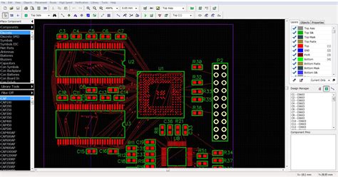
Use Gerber viewer software to visually inspect the files and check for any apparent errors. Many PCB design software packages also include Design Rule Check (DRC) tools that can help identify potential issues in the Gerber files.
9. Have the Gerber files been compressed and named appropriately?
When sending Gerber files to the PCB manufacturer, it is good practice to compress the files into a single archive (e.g., ZIP or RAR) to facilitate easy transfer and ensure that no files are missing. Naming the archive and individual Gerber files appropriately helps to prevent confusion and ensures that the manufacturer can easily identify each file’s contents.
Consider the following naming conventions:
- Include the project name or identifier in the archive name
- Use descriptive names for each Gerber file, indicating the layer type and function (e.g., “ProjectName_TopCopper.gbr” or “ProjectName_BottomSolderMask.gbr”)
- Include a README file or fabrication drawing that provides an overview of the project and any special instructions or requirements
Clear and consistent file naming, along with proper documentation, streamlines the communication process between the designer and the PCB manufacturer, reducing the likelihood of errors and misunderstandings.

FAQ
Q1: What is the difference between Extended Gerber (RS-274X) and Gerber X2 formats?
A1: Extended Gerber (RS-274X) is the most widely used Gerber file format and is supported by the majority of PCB manufacturers. It includes all the necessary information to fabricate the PCB, such as copper layers, solder mask, silkscreen, and drill data. Gerber X2 is a newer format that builds upon the RS-274X format by including additional metadata, making the files more self-contained and intelligent. This metadata can include layer types, material specifications, and design intent information, which can help streamline the communication between the designer and the manufacturer.
Q2: Why is it important to specify the layer stackup and copper weights in the Gerber files?
A2: Specifying the layer stackup and copper weights in the Gerber files is crucial because these factors directly impact the PCB’s electrical performance, impedance control, and manufacturability. The layer stackup defines the arrangement and order of the conductive layers and the dielectric materials between them, which affects the board’s signal integrity and power distribution. Copper weights, expressed in ounces per square foot, determine the thickness of the copper on each layer, influencing the current-carrying capacity and the ability to manufacture fine-pitch traces and features. By providing accurate layer stackup and copper weight information, designers enable PCB manufacturers to produce boards that meet the desired electrical and mechanical specifications.
Q3: What should I do if I encounter errors or discrepancies in my Gerber files?
A3: If you encounter errors or discrepancies in your Gerber files, the first step is to identify and understand the nature of the issue. Use Gerber viewer software to visually inspect the files and check for any apparent errors, such as missing layers, incorrect aperture definitions, or conflicting features. Many PCB design software packages also include Design Rule Check (DRC) tools that can help identify potential issues in the Gerber files. Once you have identified the issues, go back to your PCB design software and make the necessary corrections. Generate new Gerber files and review them again to ensure that the errors have been resolved. If you are unsure about how to address specific issues, consult with your PCB manufacturer or a knowledgeable colleague for guidance.
Q4: Can I use different coordinate formats for different layers in the Gerber files?
A4: While it is technically possible to use different coordinate formats for different layers in the Gerber files, it is not recommended. Using a consistent coordinate format throughout all the Gerber files is essential to ensure accurate and reliable PCB fabrication. Mixing absolute and incremental coordinates within the same set of Gerber files can lead to errors and misalignment during manufacturing, as the PCB manufacturer’s software may struggle to interpret the data correctly. To avoid potential issues, choose one coordinate format (either absolute or incremental) and use it consistently across all Gerber files for a given PCB design project.
Q5: How can I ensure that my Gerber files are compatible with my PCB manufacturer’s requirements?
A5: To ensure that your Gerber files are compatible with your PCB manufacturer’s requirements, follow these steps:
-
Consult with your PCB manufacturer early in the design process to understand their specific Gerber file requirements, such as preferred file formats, coordinate formats, and naming conventions.
-
Provide your manufacturer with a complete set of Gerber files, including all necessary layers, drill data, and any additional documentation, such as a fabrication drawing or README file.
-
Use industry-standard file formats, such as Extended Gerber (RS-274X) or Gerber X2, to ensure broad compatibility with PCB manufacturing systems.
-
Thoroughly review your Gerber files for errors and discrepancies before sending them to the manufacturer, using Gerber viewer software and design rule checks (DRC) to identify potential issues.
-
Maintain open communication with your PCB manufacturer throughout the fabrication process, addressing any questions or concerns promptly to avoid delays and misunderstandings.
By following these steps and adhering to industry best practices, you can minimize the risk of compatibility issues and ensure a smooth collaboration with your PCB manufacturer.

Conclusion
Generating accurate and complete Gerber files is essential for successful PCB fabrication. By paying close attention to the nine key considerations discussed in this article, designers can ensure that their Gerber files are free of errors, compatible with their manufacturer’s requirements, and optimized for efficient production.
Remember to include all necessary layers, use consistent coordinate formats and aperture definitions, clearly define the board outline, and provide accurate drill data. Specifying the layer stackup and copper weights, thoroughly reviewing the files for errors, and properly compressing and naming the files are also crucial steps in the Gerber file output process.
By following these guidelines and maintaining open communication with their PCB manufacturer, designers can streamline the fabrication process, reduce the risk of errors and delays, and ultimately achieve high-quality, reliable PCBs that meet their design intent.

No responses yet