Understanding Current Flow and Return Paths
When current flows through a circuit, it must always have a complete path from the source, through the load, and back to the source. This complete loop is essential for the circuit to function properly. In printed circuit boards (PCBs), the return current path is a critical aspect of the design that ensures the current has a low-impedance path to return to its source.
The Importance of a Low-Impedance Return Path
A low-impedance return path is crucial for several reasons:
-
Signal integrity: A high-impedance return path can lead to signal distortion, reflections, and crosstalk, which can compromise the performance of the circuit.
-
Electromagnetic compatibility (EMC): Poor return current paths can result in increased electromagnetic interference (EMI), which can affect the operation of nearby electronic devices and cause the circuit to fail EMC regulations.
-
Power integrity: Inadequate return paths can cause voltage drops and power supply noise, which can lead to malfunctions or even damage to components.
PCB Stackup and Return Current
The PCB stackup refers to the arrangement of copper layers and insulating materials that make up the PCB. A typical PCB stackup consists of multiple layers, including signal layers, power planes, and ground planes.
Signal Layers and Reference Planes
Signal layers are used to route the traces that carry signals between components on the PCB. These traces must have a reference plane, which is typically a ground or power plane, to provide a low-impedance return path for the current.
| Layer | Purpose |
|---|---|
| Signal Layer | Routes traces between components |
| Ground Plane | Provides a low-impedance return path for current |
| Power Plane | Distributes power to components and can also serve as a reference plane |
The Role of Ground Planes
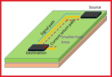
Ground planes play a crucial role in providing a low-impedance return path for the current. By placing a ground plane adjacent to a signal layer, the return current can flow directly beneath the signal trace, minimizing the loop area and reducing inductance.
Benefits of using a ground plane:
- Reduces impedance
- Minimizes loop area
- Decreases inductance
- Improves signal integrity
- Helps with EMI shielding
High-Speed Signals and Return Current
As the speed of signals in PCBs increases, the return current path becomes even more critical. High-speed signals are more susceptible to signal integrity issues caused by poor return paths.
The Skin Effect
At high frequencies, current tends to flow on the surface of conductors due to the skin effect. This phenomenon causes the effective resistance of the conductor to increase, leading to greater signal attenuation and distortion.
To mitigate the skin effect, designers must ensure that the return current path is as close to the signal trace as possible. This proximity helps to minimize the loop area and reduces the inductance of the return path.
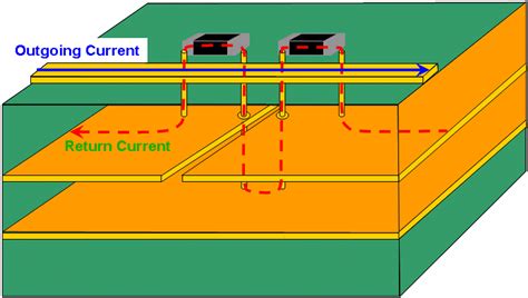
Discontinuities in the Return Path
Discontinuities in the return path, such as gaps in the ground plane or signal traces crossing split planes, can cause significant problems for high-speed signals. These discontinuities create a high-impedance point in the return path, leading to reflections, crosstalk, and EMI.
To avoid discontinuities, designers should:
- Minimize the number of splits in the reference plane
- Use stitching capacitors or vias to bridge gaps in the reference plane
- Route signals over a continuous reference plane whenever possible

Designing for Proper Return Current Paths
When designing a PCB, it is essential to consider the return current path from the beginning. By following best practices and guidelines, designers can ensure that their PCBs have low-impedance return paths, minimizing signal integrity issues and EMI.
Routing Guidelines
- Route signals over a continuous reference plane
- Avoid routing signals over split planes or gaps in the reference plane
- Use stitching capacitors or vias to bridge gaps when necessary
- Minimize the loop area by keeping the signal trace close to its reference plane
- Use a ground plane adjacent to signal layers to provide a low-impedance return path
Stackup Design
- Use a balanced stackup with alternating signal and reference layers
- Place ground planes adjacent to signal layers to minimize loop area and inductance
- Use a sufficient number of ground and power planes to ensure low-impedance return paths
- Consider the use of shielding layers for sensitive signals or to reduce EMI
Decoupling Capacitors
Decoupling capacitors play a crucial role in maintaining power integrity and providing a local, low-impedance return path for high-frequency currents. Place decoupling capacitors close to the power pins of ICs to minimize the loop area and reduce the inductance of the return path.
| Capacitor Value | Frequency Range |
|---|---|
| 0.1 μF | 10 kHz – 1 MHz |
| 0.01 μF | 1 MHz – 10 MHz |
| 1000 pF | 10 MHz – 100 MHz |
| 100 pF | 100 MHz – 1 GHz |
Ground Stitching
When a signal must cross a gap in the reference plane, use stitching vias or capacitors to provide a low-impedance path for the return current. Stitching helps to minimize the discontinuity in the return path and reduces the risk of signal integrity issues and EMI.
FAQ
Q1: What is the return current path in a PCB?
A1: The return current path in a PCB is the low-impedance path that allows current to flow back to its source after passing through a load. It is essential for maintaining signal integrity, power integrity, and electromagnetic compatibility.
Q2: Why is a low-impedance return path important?
A2: A low-impedance return path is important because it minimizes signal distortion, reflections, and crosstalk. It also reduces electromagnetic interference (EMI) and ensures proper power distribution to components.
Q3: What is the role of ground planes in providing a return current path?
A3: Ground planes provide a low-impedance return path for current by allowing the return current to flow directly beneath the signal trace. This proximity minimizes the loop area and reduces inductance, improving signal integrity and reducing EMI.
Q4: How does the skin effect impact high-speed signals and return current?
A4: The skin effect causes high-frequency currents to flow on the surface of conductors, increasing the effective resistance and leading to signal attenuation and distortion. To mitigate this effect, the return current path should be as close to the signal trace as possible, minimizing the loop area and inductance.
Q5: What are some best practices for designing proper return current paths in PCBs?
A5: Some best practices include routing signals over continuous reference planes, minimizing splits in the reference plane, using stitching capacitors or vias to bridge gaps, minimizing loop area by keeping signal traces close to reference planes, using a balanced stackup, placing decoupling capacitors close to IC power pins, and using ground stitching when signals must cross gaps in the reference plane.
Conclusion
Designing proper return current paths is a critical aspect of PCB design that ensures signal integrity, power integrity, and electromagnetic compatibility. By understanding the principles of current flow, the role of reference planes, and the impact of high-speed signals, designers can create PCBs with low-impedance return paths that minimize signal distortion, reflections, crosstalk, and EMI.
Following best practices such as using a balanced stackup, placing ground planes adjacent to signal layers, minimizing splits in the reference plane, and using stitching capacitors or vias when necessary, designers can create robust and reliable PCBs that perform well in a variety of applications.
As the demand for high-speed, high-performance electronic devices continues to grow, the importance of proper return current path design will only increase. By staying up-to-date with the latest techniques and guidelines, PCB designers can ensure that their boards meet the evolving needs of the industry and provide reliable, efficient, and cost-effective solutions for their clients.
No responses yet