Introduction to PCB Conductive Ink Printing
Printed circuit boards (PCBs) are essential components in modern electronics, providing the foundation for interconnecting electronic components. Traditional PCB manufacturing methods involve subtractive processes, such as etching copper from a substrate. However, recent advancements in additive manufacturing, particularly 3D printing technology, have opened up new possibilities for PCB fabrication. One promising approach is the use of conductive ink printing in 3D printers to create PCBs. In this article, we will explore what PCB designers need to know about conductive ink printing 3D printers and how this technology can revolutionize the PCB industry.
Understanding Conductive Ink Printing Technology
What is Conductive Ink?
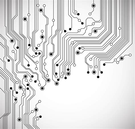
Conductive ink is a specialized material that contains conductive particles, such as silver, copper, or graphene, suspended in a liquid medium. When the ink is printed onto a substrate and cured, it forms a conductive pathway that allows electrical current to flow through it. Conductive inks have been used in various applications, including printed electronics, flexible circuits, and RFID antennas.
How Does Conductive Ink Printing Work in 3D Printers?
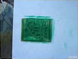
Conductive ink printing in 3D printers involves depositing conductive ink onto a substrate layer by layer to create a three-dimensional structure. The process typically uses inkjet printing technology, where the conductive ink is precisely dispensed through a printhead onto the substrate. The printer follows a digital design file, such as a Gerber file, to accurately place the conductive traces and components on the PCB.
After each layer is printed, the ink is cured using heat or UV light to solidify and achieve the desired conductivity. This process is repeated until the complete PCB is formed. Some 3D printers also have the capability to print insulating materials alongside the conductive ink, allowing for the creation of multi-layer PCBs.
Advantages of Conductive Ink Printing 3D Printers for PCB Design
Rapid Prototyping and Iteration
One of the key advantages of using conductive ink printing 3D printers for PCB design is the ability to rapidly prototype and iterate designs. Traditional PCB manufacturing methods often require long lead times and can be costly for small batch productions. With 3D printing, designers can quickly print and test their PCB designs, making it easier to identify and fix issues early in the development process. This iterative approach can significantly reduce time-to-market and development costs.
Customization and Flexibility
Conductive ink printing 3D printers offer a high degree of customization and flexibility in PCB design. Unlike traditional manufacturing methods that rely on standard PCB sizes and layouts, 3D printing allows designers to create custom-shaped PCBs and integrate complex geometries. This opens up new possibilities for innovative PCB designs that can be optimized for specific applications or space constraints.
Moreover, 3D printing enables the creation of flexible and stretchable PCBs by using flexible substrates and conductive inks. This is particularly useful for wearable electronics, medical devices, and other applications that require conformable or bendable circuits.
Cost-Effective Low-Volume Production
For low-volume production runs, conductive ink printing 3D printers can be a cost-effective alternative to traditional PCB manufacturing methods. Setup costs and tooling fees associated with conventional PCB fabrication can be significant, making it uneconomical for small batches. With 3D printing, there are no setup costs, and the price per PCB remains relatively constant regardless of the quantity produced. This makes it an attractive option for prototyping, limited-run productions, and niche applications.

Challenges and Considerations for PCB Designers
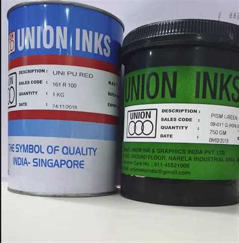
Material Selection and Conductivity
When designing PCBs for conductive ink printing, material selection is crucial. The choice of conductive ink and substrate material will impact the PCB’s performance, durability, and cost. PCB designers need to consider the conductivity of the ink, as well as its adhesion properties and compatibility with the substrate. The conductivity of printed traces may be lower compared to traditional copper traces, which can affect signal integrity and power handling capabilities.
Designers should work closely with 3D printing service providers or material suppliers to select the appropriate conductive ink and substrate combination for their specific application requirements.
Design Rules and Limitations
PCB designers need to be aware of the design rules and limitations associated with conductive ink printing 3D printers. The resolution and accuracy of the printed traces may be lower compared to traditional PCB manufacturing methods. Designers should consider the minimum feature sizes, trace widths, and spacing that can be reliably achieved with the specific 3D printer and ink combination.
Additionally, designers should account for the layer thickness and the number of layers that can be printed. The thickness of the printed layers can impact the overall PCB thickness and the ability to create vias and interconnects between layers.
Post-Processing and Assembly
After printing, PCBs may require post-processing steps to improve their performance and durability. This can include sintering, which involves heating the printed traces to enhance their conductivity and mechanical strength. Designers should be aware of the post-processing requirements and factor them into the design and production timeline.
Assembly of components onto 3D printed PCBs may also present challenges. The surface finish and solderability of printed traces can differ from traditional PCBs, requiring adjustments to the assembly process. Designers should collaborate with the assembly team to ensure compatibility and reliability of the final product.
Future Trends and Opportunities
Multi-Material 3D Printing
One exciting area of development in conductive ink printing 3D printers is multi-material printing. This involves the ability to print multiple materials, such as conductive inks, insulating materials, and even functional components, in a single print job. Multi-material printing opens up new possibilities for creating complex, integrated electronic devices with embedded sensors, antennas, and other features.
Hybrid Manufacturing Approaches
Another trend is the combination of conductive ink printing with other manufacturing technologies, such as traditional PCB fabrication or injection molding. Hybrid manufacturing approaches can leverage the strengths of each technology to create high-performance, cost-effective solutions. For example, a 3D printed PCB with conductive ink traces could be integrated with a conventionally manufactured PCB to form a hybrid board with enhanced functionality.
Sustainability and Environmental Benefits
Conductive ink printing 3D printers also offer potential sustainability and environmental benefits compared to traditional PCB manufacturing methods. The additive nature of 3D printing minimizes material waste, as conductive ink is only deposited where needed. Additionally, some conductive inks are formulated using eco-friendly, non-toxic materials, reducing the environmental impact of PCB production.
Frequently Asked Questions (FAQ)
1. What is the typical conductivity of printed traces compared to copper traces?
The conductivity of printed traces using conductive inks is generally lower than that of copper traces. The exact conductivity depends on the specific ink formulation and printing process used. Typical values range from 10% to 50% of the conductivity of bulk copper. However, advancements in conductive ink technology are continually improving the achievable conductivity levels.
2. Can 3D printed PCBs be used for high-frequency applications?
Yes, 3D printed PCBs can be used for high-frequency applications, but designers need to consider the limitations and characteristics of the conductive ink and substrate materials. The lower conductivity and potentially higher surface roughness of printed traces can impact signal integrity at high frequencies. Proper design techniques, such as impedance matching and shielding, should be employed to mitigate these effects.
3. Are there any size limitations for PCBs produced by conductive ink printing 3D printers?
The size limitations for PCBs produced by conductive ink printing 3D printers depend on the specific printer and its build volume. Some desktop 3D printers have build volumes ranging from a few centimeters to several inches, while industrial-scale printers can accommodate larger PCB sizes. It’s important to consult the specifications of the particular 3D printer being used to determine the maximum PCB dimensions that can be produced.
4. How do the costs of 3D printed PCBs compare to traditionally manufactured PCBs?
The cost comparison between 3D printed PCBs and traditionally manufactured PCBs varies depending on factors such as the PCB complexity, quantity, and turnaround time. For low-volume production and prototyping, 3D printed PCBs can be more cost-effective due to the absence of setup costs and tooling fees. However, for high-volume production, traditional PCB manufacturing methods may offer lower per-unit costs due to economies of scale.
5. Can 3D printed PCBs be used in harsh environments or extreme conditions?
The suitability of 3D printed PCBs for harsh environments or extreme conditions depends on the materials used and the post-processing techniques applied. Some conductive inks and substrate materials are designed to withstand high temperatures, moisture, or chemical exposure. However, the durability and reliability of 3D printed PCBs in extreme conditions may not match that of traditionally manufactured PCBs. Thorough testing and validation should be conducted to ensure the performance and reliability of 3D printed PCBs in the intended operating environment.
Conclusion
Conductive ink printing 3D printers offer exciting opportunities for PCB designers to innovate and streamline the PCB development process. With the ability to rapidly prototype, create custom designs, and produce low-volume runs cost-effectively, this technology has the potential to transform the PCB industry. However, designers must also be aware of the challenges and considerations associated with conductive ink printing, such as material selection, design rules, and post-processing requirements.
As the technology continues to evolve, with advancements in multi-material printing and hybrid manufacturing approaches, the capabilities of conductive ink printing 3D printers will expand further. PCB designers who stay informed about these developments and adapt their design strategies accordingly will be well-positioned to leverage the benefits of this innovative technology.
By understanding the principles, advantages, and limitations of conductive ink printing 3D printers, PCB designers can make informed decisions and push the boundaries of what is possible in PCB design and manufacturing. The future of PCBs looks bright, with conductive ink printing 3D printers playing an increasingly important role in shaping the electronics landscape.
No responses yet