Introduction to PCB Stack-up
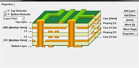
A printed circuit board (PCB) stack-up refers to the arrangement of copper and insulating layers that make up a PCB. The stack-up defines the number of layers, their order, and the thickness of each layer. Choosing the right PCB stack-up is crucial for ensuring proper functionality, signal integrity, and manufacturability of the board.
In this article, we will focus on the basic stack-up of a 16-layer PCB and discuss its various aspects, including layer arrangement, materials used, and design considerations.
16 Layer PCB Stack-up Overview
A 16-layer PCB is a complex, high-density board that is commonly used in advanced electronic applications such as telecommunications, aerospace, and medical devices. The increased number of layers allows for greater routing density, better signal integrity, and improved power distribution.
A typical 16-layer PCB stack-up consists of the following layers:
| Layer | Description |
|---|---|
| Top Layer | Signal layer, component placement |
| Ground Plane | Ground reference for top layer signals |
| Signal Layer 1 | Inner signal layer |
| Signal Layer 2 | Inner signal layer |
| Power Plane 1 | Power distribution layer |
| Ground Plane | Ground reference for power plane and inner signals |
| Signal Layer 3 | Inner signal layer |
| Signal Layer 4 | Inner signal layer |
| Signal Layer 5 | Inner signal layer |
| Signal Layer 6 | Inner signal layer |
| Ground Plane | Ground reference for inner signals |
| Power Plane 2 | Power distribution layer |
| Signal Layer 7 | Inner signal layer |
| Signal Layer 8 | Inner signal layer |
| Bottom Layer | Signal layer, component placement |

Materials Used in 16 Layer PCB Stack-up
The choice of materials used in a 16-layer PCB stack-up is critical for ensuring the board’s performance and reliability. The most common materials used are:
Copper Foil
Copper foil is used for the conductive layers of the PCB. The thickness of the copper foil is typically expressed in ounces per square foot (oz/ft²). For a 16-layer PCB, the standard copper thickness is 1 oz/ft² (35 µm) for the outer layers and 0.5 oz/ft² (17.5 µm) for the inner layers.
Dielectric Material
The dielectric material is used as an insulator between the conductive layers. The most common dielectric materials used in 16-layer PCBs are:
-
FR-4: A composite material made of woven fiberglass cloth with an epoxy resin binder. FR-4 is the most widely used dielectric material due to its good mechanical and electrical properties, as well as its cost-effectiveness.
-
High-Tg FR-4: A variant of FR-4 with a higher glass transition temperature (Tg), which improves the material’s thermal stability and reduces the risk of delamination during the assembly process.
-
Isola 370HR: A high-performance dielectric material with low loss and high thermal resistance, making it suitable for high-speed applications.
The thickness of the dielectric material varies depending on the desired characteristic impedance and the spacing between the layers.

16 Layer PCB Stack-up Design Considerations
When designing a 16-layer PCB stack-up, several factors must be considered to ensure optimal performance and manufacturability:
Signal Integrity
Signal integrity refers to the quality of the electrical signals transmitted through the PCB. To maintain signal integrity, the following guidelines should be followed:
- Keep signal traces as short as possible to minimize losses and reflections.
- Maintain consistent characteristic impedance throughout the signal path.
-
Use proper grounding and shielding techniques to reduce noise and crosstalk.
-
Route high-speed signals on inner layers, sandwiched between ground planes, to minimize electromagnetic interference (EMI).
Power Distribution
Proper power distribution is essential for ensuring the stable operation of the components on the PCB. When designing the power distribution network in a 16-layer PCB, consider the following:
- Use dedicated power planes to provide low-impedance power distribution to the components.
- Place power planes close to the ground planes to minimize inductance and provide better decoupling.
- Use multiple power planes for different voltage levels, if required.
- Implement proper decoupling techniques, such as placing decoupling capacitors close to the power pins of the components.
Thermal Management
With the increasing power density in modern electronic devices, thermal management becomes a critical factor in PCB design. To ensure proper heat dissipation in a 16-layer PCB, consider the following:
- Use thermally conductive dielectric materials, such as Isola 370HR, to improve heat transfer between layers.
- Incorporate thermal vias to conduct heat from the components to the inner layers and the opposite side of the board.
- Use large copper pours on the outer layers to help dissipate heat.
Manufacturability
Designing a 16-layer PCB stack-up that is easy to manufacture can help reduce costs and improve reliability. Some key factors to consider include:
- Ensure that the stack-up is symmetrical to minimize warpage during the manufacturing process.
- Use standard layer thicknesses and materials whenever possible to reduce lead times and costs.
- Follow the manufacturer’s design guidelines for minimum trace widths, spacing, and via sizes.

Example of a 16 Layer PCB Stack-up
Here is an example of a 16-layer PCB stack-up with a total thickness of 1.6 mm:
| Layer | Material | Thickness (mm) |
|---|---|---|
| Top Layer | 1 oz/ft² copper | 0.035 |
| Prepreg | FR-4 | 0.1 |
| Ground Plane | 0.5 oz/ft² copper | 0.0175 |
| Core | FR-4 | 0.2 |
| Signal Layer 1 | 0.5 oz/ft² copper | 0.0175 |
| Prepreg | FR-4 | 0.1 |
| Signal Layer 2 | 0.5 oz/ft² copper | 0.0175 |
| Core | FR-4 | 0.2 |
| Power Plane 1 | 0.5 oz/ft² copper | 0.0175 |
| Prepreg | FR-4 | 0.1 |
| Ground Plane | 0.5 oz/ft² copper | 0.0175 |
| Core | FR-4 | 0.2 |
| Signal Layer 3 | 0.5 oz/ft² copper | 0.0175 |
| Prepreg | FR-4 | 0.1 |
| Signal Layer 4 | 0.5 oz/ft² copper | 0.0175 |
| Core | FR-4 | 0.2 |
| Signal Layer 5 | 0.5 oz/ft² copper | 0.0175 |
| Prepreg | FR-4 | 0.1 |
| Signal Layer 6 | 0.5 oz/ft² copper | 0.0175 |
| Core | FR-4 | 0.2 |
| Ground Plane | 0.5 oz/ft² copper | 0.0175 |
| Prepreg | FR-4 | 0.1 |
| Power Plane 2 | 0.5 oz/ft² copper | 0.0175 |
| Core | FR-4 | 0.2 |
| Signal Layer 7 | 0.5 oz/ft² copper | 0.0175 |
| Prepreg | FR-4 | 0.1 |
| Signal Layer 8 | 0.5 oz/ft² copper | 0.0175 |
| Prepreg | FR-4 | 0.1 |
| Bottom Layer | 1 oz/ft² copper | 0.035 |
In this example, the stack-up uses a combination of core and prepreg layers to achieve the desired thickness and ensure proper bonding between the layers. The signal layers are symmetrically distributed, with ground and power planes strategically placed to maintain signal integrity and provide stable power distribution.
FAQ
1. What is the advantage of using a 16-layer PCB over a PCB with fewer layers?
A 16-layer PCB offers several advantages over PCBs with fewer layers:
- Higher routing density: The increased number of layers allows for more complex routing and a higher component density.
- Better signal integrity: With more layers, signals can be routed on inner layers, sandwiched between ground planes, which reduces crosstalk and EMI.
- Improved power distribution: Dedicated power planes can provide stable power to components, and the increased number of layers allows for better decoupling.
2. Can I use different dielectric materials in the same 16-layer PCB stack-up?
Yes, it is possible to use different dielectric materials in the same 16-layer PCB stack-up. For example, you may use a high-performance material like Isola 370HR for the high-speed signal layers and standard FR-4 for the other layers. However, mixing materials can increase the complexity and cost of the manufacturing process, so it should only be done when necessary.
3. How does the thickness of the copper foil affect the performance of a 16-layer PCB?
The thickness of the copper foil affects both the electrical and thermal performance of a 16-layer PCB:
- Electrical performance: Thicker copper foil has lower resistance, which can help reduce signal losses and improve power distribution. However, thicker copper can also increase the capacitance between layers, which may impact signal integrity.
- Thermal performance: Thicker copper foil can help dissipate heat more effectively, which is important for high-power components.
4. What is the minimum trace width and spacing for a 16-layer PCB?
The minimum trace width and spacing for a 16-layer PCB depend on several factors, including the copper thickness, the dielectric material, and the manufacturing capabilities of the PCB fabricator. As a general guideline, for a 16-layer PCB with 0.5 oz/ft² copper on the inner layers, the minimum trace width and spacing is typically around 0.1 mm (4 mil). However, it is essential to consult with the PCB fabricator to determine the specific design rules for your project.
5. How do I ensure proper signal integrity in a 16-layer PCB?
To ensure proper signal integrity in a 16-layer PCB, follow these guidelines:
- Route high-speed signals on inner layers, sandwiched between ground planes, to minimize crosstalk and EMI.
- Maintain consistent characteristic impedance throughout the signal path by controlling the trace width, thickness, and spacing to the reference plane.
- Keep signal traces as short as possible to minimize losses and reflections.
- Use proper termination techniques, such as series termination or differential pair routing, when necessary.
- Implement proper grounding and shielding techniques, such as using ground vias and copper pours, to reduce noise and crosstalk.
Conclusion
Designing a 16-layer PCB stack-up requires careful consideration of various factors, including signal integrity, power distribution, thermal management, and manufacturability. By understanding the basic structure of a 16-layer PCB and following best design practices, you can create a stack-up that meets the performance requirements of your application while ensuring reliable and cost-effective manufacturing.
When designing a 16-layer PCB stack-up, it is essential to work closely with your PCB fabricator to ensure that your design is compatible with their manufacturing capabilities and design rules. By collaborating with experienced professionals and staying up to date with the latest industry standards and guidelines, you can successfully navigate the complexities of 16-layer PCB design and bring your high-performance electronic products to market.
No responses yet