Introduction to Tenting Via
In the world of printed circuit board (PCB) fabrication, tenting via is a crucial process THAt ensures the reliability and functionality of the final product. Vias are small holes drilled through the PCB to connect different layers of the board electrically. Tenting via involves covering these holes with a thin layer of solder mask, which protects the vias from damage and improves the overall quality of the PCB.
What is a Via?
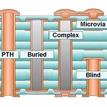
A via is a small hole drilled through a PCB to create an electrical connection between different layers of the board. Vias are essential in PCB design as they allow for the creation of complex circuits and the efficient use of space on the board. There are several types of vias, including:
- Through hole vias: These vias go through the entire thickness of the PCB and are typically used for components with leads that need to be soldered to the board.
- Blind vias: These vias start on an outer layer of the PCB and terminate on an inner layer, but do not go through the entire board.
- Buried vias: These vias are located entirely within the inner layers of the PCB and do not extend to the outer layers.
What is Tenting Via?
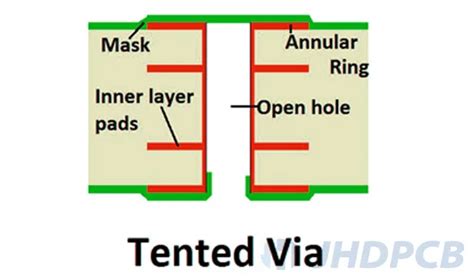
Tenting via is the process of covering the vias on a PCB with a thin layer of solder mask. The solder mask is a protective coating that is applied to the surface of the PCB to prevent solder bridging and short circuits. When a via is tented, the solder mask covers the hole completely, creating a smooth surface on the top and bottom of the board.
There are two main methods for tenting vias:
-
Liquid Photo Imageable (LPI) solder mask: This method involves applying a liquid solder mask to the surface of the PCB and then exposing it to UV light through a photomask. The areas of the solder mask that are exposed to light harden, while the unexposed areas remain liquid and can be washed away. This process allows for precise control over the placement of the solder mask and can be used to tent vias selectively.
-
Dry film solder mask: This method involves applying a dry film of solder mask to the surface of the PCB and then exposing it to UV light through a photomask. The areas of the solder mask that are exposed to light harden, while the unexposed areas remain soft and can be peeled away. This process is faster and more cost-effective than LPI solder mask but does not allow for as much precision in the placement of the solder mask.
Advantages of Tenting Via
Tenting via offers several advantages in PCB fabrication, including:
Improved Reliability
One of the primary benefits of tenting via is improved reliability of the PCB. When a via is left untented, it is exposed to the environment and can be damaged by moisture, dust, or other contaminants. Over time, this can lead to corrosion or other issues that can cause the via to fail, resulting in a malfunctioning PCB.
By covering the via with a layer of solder mask, tenting via helps to protect the via from damage and ensures that it remains functional over the life of the PCB. This is particularly important in harsh environments where the PCB may be exposed to high temperatures, humidity, or other challenging conditions.
Better Solderability
Tenting via can also improve the solderability of the PCB. When a via is left untented, solder can flow into the hole during the soldering process, creating a weak joint that is prone to failure. By covering the via with solder mask, tenting via prevents solder from flowing into the hole and ensures a stronger, more reliable solder joint.
This is particularly important in high-density PCBs where there are many vias in close proximity to each other. Without tenting via, there is a risk of solder bridging between adjacent vias, which can cause short circuits and other issues.
Improved Aesthetics
Tenting via can also improve the aesthetics of the PCB. When a via is left untented, it can be visible on the surface of the board, which can detract from the overall appearance of the PCB. By covering the via with solder mask, tenting via creates a smooth, uniform surface that looks more professional and polished.
This is particularly important in consumer electronics and other applications where the appearance of the PCB is important. A well-tented PCB can help to create a high-quality, premium look and feel that enhances the overall appeal of the product.
Cost Savings
Tenting via can also offer cost savings in PCB fabrication. When a via is left untented, it requires additional processing steps to ensure that it is protected from damage and remains functional. This can add time and cost to the fabrication process.
By tenting the via during the Solder Mask Application process, these additional steps can be eliminated, reducing the overall cost of fabrication. This is particularly important in high-volume production runs where even small cost savings can add up to significant amounts over time.
Challenges of Tenting Via
While tenting via offers many advantages in PCB fabrication, there are also some challenges that must be considered.
Difficulty in Inspection
One of the main challenges of tenting via is the difficulty in inspecting the vias after the solder mask has been applied. Because the vias are covered by the solder mask, it can be difficult to see if there are any issues with the vias, such as poor plating or incomplete filling.
This can be particularly problematic in high-reliability applications where even small defects in the vias can cause significant issues. In these cases, additional inspection techniques may be required, such as x-ray inspection or destructive testing.
Limitations in Via Size
Another challenge of tenting via is the limitations in via size that can be accommodated. Because the solder mask must completely cover the via, there is a limit to how small the via can be while still allowing for effective tenting.
This can be a problem in high-density PCBs where there are many small vias in close proximity to each other. In these cases, alternative techniques may be required, such as via-in-pad or microvias, which allow for smaller via sizes.
Potential for Void Formation
Finally, there is a potential for void formation in tented vias, particularly in high-aspect-ratio vias. When the solder mask is applied to the via, there is a risk of trapping air or other gases in the via, which can lead to the formation of voids.
These voids can weaken the mechanical and electrical integrity of the via and can lead to reliability issues over time. To mitigate this risk, careful process control and optimization is required, including the use of vacuum impregnation or other techniques to remove trapped gases from the vias.

Best Practices for Tenting Via
To ensure the best results when tenting via, there are several best practices that should be followed:
Choose the Right Solder Mask
Choosing the right solder mask is critical for effective tenting via. The solder mask should have good flow properties to ensure that it completely fills the via without leaving any voids or gaps. It should also have good adhesion to the PCB surface and the via walls to ensure a strong, reliable bond.
Optimize the Solder Mask Application Process
The solder mask application process should be carefully optimized to ensure the best results. This includes controlling the thickness of the solder mask, the exposure time and intensity, and the development and curing processes.
It is also important to ensure that the solder mask is applied evenly and consistently across the entire PCB surface to avoid any areas of weakness or vulnerability.
Use Appropriate Via Fill Materials
In some cases, it may be necessary to use via fill materials in addition to tenting via to ensure the best results. Via fill materials are used to fill the via completely before the solder mask is applied, creating a solid, stable base for the solder mask to adhere to.
There are several types of via fill materials available, including conductive and non-conductive epoxies, as well as metal-filled materials such as copper or silver. The choice of via fill material will depend on the specific requirements of the application, including the electrical and thermal properties required.
Conduct Thorough Inspection and Testing
Finally, it is important to conduct thorough inspection and testing of the PCB after the tenting via process is complete. This includes visual inspection to ensure that the solder mask has been applied evenly and consistently, as well as electrical testing to ensure that the vias are functioning properly.
In some cases, additional testing may be required, such as x-ray inspection or destructive testing, to ensure that there are no hidden defects or issues with the vias.
FAQs
1. What is the difference between tented and untented vias?
Tented vias are covered with a layer of solder mask, while untented vias are left exposed. Tented vias offer improved reliability, solderability, and aesthetics, while untented vias are more vulnerable to damage and can be more difficult to solder.
2. Can all vias be tented?
Not all vias can be tented effectively. Very small vias or high-aspect-ratio vias may be difficult to tent completely, and alternative techniques such as via-in-pad or microvias may be required.
3. What are the most common methods for tenting vias?
The two most common methods for tenting vias are liquid photo imageable (LPI) solder mask and dry film solder mask. LPI solder mask offers more precision and control, while dry film solder mask is faster and more cost-effective.
4. How does tenting via improve the reliability of a PCB?
Tenting via improves the reliability of a PCB by protecting the vias from damage and contamination, preventing solder from flowing into the via during the soldering process, and creating a stronger, more stable solder joint.
5. What are some of the challenges of tenting via?
Some of the challenges of tenting via include difficulty in inspecting the vias after the solder mask has been applied, limitations in via size that can be accommodated, and the potential for void formation in high-aspect-ratio vias. Careful process control and optimization can help to mitigate these challenges.
Conclusion
Tenting via is a critical process in PCB fabrication that offers many advantages, including improved reliability, better solderability, improved aesthetics, and cost savings. By covering the vias with a layer of solder mask, tenting via helps to protect the vias from damage and contamination, ensures a stronger and more reliable solder joint, and creates a smooth, uniform surface that enhances the overall appearance of the PCB.
However, tenting via also presents some challenges, including difficulty in inspection, limitations in via size, and the potential for void formation. To ensure the best results, it is important to choose the right solder mask, optimize the solder mask application process, use appropriate via fill materials, and conduct thorough inspection and testing.
By following these best practices and carefully considering the specific requirements of the application, PCB manufacturers can effectively utilize tenting via to create high-quality, reliable PCBs that meet the needs of even the most demanding applications.
No responses yet