How Does Surface-Mount Technology Work?
In surface-mount technology, the components are mounted directly onto copper pads on the surface of the printed circuit board instead of being inserted into holes that go through the board. The component leads are soldered onto these pads to form electrical and mechanical connections. SMT components are usually smaller than their through-hole counterparts because they have smaller leads or no leads at all.
The main steps in the SMT assembly process are:
- Solder paste printing: A thin layer of solder paste (a mixture of tiny solder balls and flux) is applied to the PCB pads using a stencil.
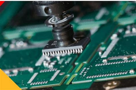
- Component placement: The surface-mount components are precisely placed onto their pads on the PCB. This is usually done by automated pick-and-place machines.
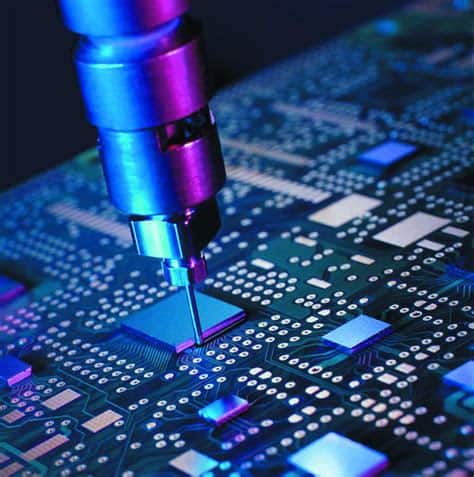
- Reflow soldering: The populated PCB goes through a reflow oven. The solder in the solder paste melts in a controlled way, creating permanent solder joints.
- Inspection and testing: The assembled PCBs are inspected and tested to ensure the solder joints are good and the board functions properly.
Advantages of Surface-Mount Technology
SMT offers several advantages over through-hole mounting:
- Smaller components and higher component density, enabling smaller PCBs
- Faster and more automated assembly
- Lower cost due to faster assembly and less drilling
- Better mechanical performance under shake and vibration conditions
- Fewer unwanted RF signal effects and better EMC performance due to smaller component packages
Disadvantages of Surface-Mount Technology
However, SMT also has some disadvantages compared to through-hole technology:
- Manual prototype assembly and component-level repair is more difficult and requires skilled operators and specialized tools
- SMT may not be suitable for high-power applications that require heat sinks
- Components can be knocked off the board more easily before soldering
- Solder joint quality is highly dependent on the solder paste printing process
- X-ray machines may be needed to inspect solder joints underneath packages
Surface-Mount Components
Surface-mount components are available in a wide variety of package types and sizes. Some of the most common types are:
| Package Type | Description | Typical Size Range |
|---|---|---|
| Chip | Small, rectangular blocks with metallized terminals on two sides | 0201 to 2512 |
| SOT | Small-outline transistor packages with gull-wing leads | SOT-23 to SOT-223 |
| QFP | Quad flat packages with gull-wing leads on four sides | LQFP-32 to LQFP-256 |
| BGA | Ball grid array packages with solder balls on the bottom | BGA-36 to BGA-1156 |
| CSP | Chip-scale packages not much larger than the semiconductor die | WLCSP-16 to WLCSP-144 |
The size of chip components is indicated by a 4-digit code where the first two digits represent the length and the last two digits represent the width in hundredths of an inch. For example, an 0805 chip is 0.08 inch long by 0.05 inch wide.
Packaged SMT components often have their pins formed into gull-wing shapes which extend out from the component body and bend down to touch the PCB pads. The pitch (distance between pins) can range from around 1mm (0.04 in) down to 0.4mm (0.016 in) or less for fine-pitch components.
SMT Assembly Equipment
The key pieces of equipment used in a typical SMT assembly line are:
Solder Paste Printer
A solder paste printer applies solder paste to the PCB pads through holes in a stainless steel stencil using a squeegee blade. The stencil thickness and aperture sizes control the amount of solder paste deposited.
Solder paste printers usually have an automatic vision system to align the stencil to the PCB. They also have facilities for automatic stencil cleaning.
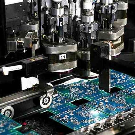
Pick-and-Place Machine
A pick-and-place (P&P) machine picks up components from feeders or trays and places them onto their pads on the PCB with high speed and precision. It uses a vacuum nozzle or gripper to pick up the components and a positioning system to place them accurately.
Modern P&P machines have multiple placement heads and can place tens of thousands of components per hour. They use vision systems to inspect the components before picking and after placing.
Reflow Oven
A reflow oven heats up the PCB assembly in a controlled way to melt the solder paste and form solder joints. It has multiple heating zones that follow a specific temperature profile suitable for the solder paste being used.
The reflow process usually takes place in an inert nitrogen atmosphere to prevent oxidation of the solder joints. The oven may also have a cooling zone at the end to cool the PCBs in a controlled way.
Inspection Systems
Various inspection systems are used to check the quality of the solder paste printing, component placement and solder joints. These include:
- Solder paste inspection (SPI) systems which use 2D or 3D vision to measure the volume and position of solder paste deposits
- Automated optical inspection (AOI) systems which use cameras and image analysis to check for missing or misplaced components and solder defects
- X-ray inspection systems which can see solder joints hidden under components like BGAs
- In-circuit test (ICT) systems which use probes and electrical tests to verify the interconnections and values of components on the board

SMT Design Considerations
Designing a PCB for surface-mount assembly requires following some guidelines to ensure manufacturability, reliability and cost-effectiveness. Some key design considerations are:
Component Selection
- Choose components that are readily available in surface-mount packages
- Avoid mixing through-hole and surface-mount components unless necessary
- Use standard component footprints from vendor datasheets or PCB Design tool libraries
- Consider the component size, pitch and placement clearances for your assembly process
PCB Layout
- Place components on a grid to allow efficient solder paste printing and pick-and-place
- Provide adequate spacing between components for solder paste printing and visual inspection
- Orient components in the same direction where possible to minimize placement head rotations
- Avoid placing components under overhanging parts like connectors
- Place fiducials on the PCB to allow vision alignment of the Solder paste stencil, P&P machine and inspection systems
Solder Paste Stencil Design
- Size the stencil apertures to deposit the right amount of solder paste on each pad
- Provide clearance between pads and apertures to prevent solder bridges
- Avoid long, narrow apertures that could cause stencil buckling
- Specify the right stencil thickness and material for the solder paste and components used
Reflow Profile Development
- Follow the solder paste manufacturer’s recommendations for reflow profile parameters like soak time, peak temperature and time above liquidus
- Use a profile that minimizes the risk of thermal damage to components while ensuring good solder joint quality
- Verify the profile on actual PCB assemblies using thermocouples and visual inspection
Frequently Asked Questions
1. What is the difference between surface-mount technology (SMT) and through-hole technology (THT)?
In SMT, components are mounted directly onto pads on the surface of the PCB, while in THT, component leads are inserted into holes that go through the PCB and are soldered on the opposite side. SMT allows for smaller components, higher density and faster assembly compared to THT.
2. Can SMT and THT components be used on the same PCB?
Yes, SMT and THT components can be mixed on the same PCB. This is often done for components that are not available in SMT packages or that require additional mechanical strength, such as connectors or large capacitors. However, mixed assembly requires extra steps and may increase cost.
3. What are the most common SMT component package types?
The most common SMT component package types are chip resistors and capacitors, small-outline transistors (SOT), quad flat packages (QFP), ball grid arrays (BGA) and chip-scale packages (CSP). Each type has its own size, lead configuration and mounting requirements.
4. How small can SMT components be?
The smallest SMT chip components commonly used are 0201 size (0.02 x 0.01 inches). Smaller sizes like 01005 (0.016 x 0.008 inches) are also available but are more challenging to handle and place. The smallest ball pitch for BGA Packages can be 0.3mm or less.
5. What are the key steps in the SMT assembly process?
The key steps in the SMT assembly process are:
- Solder paste printing: applying solder paste to the PCB pads through a stencil
- Component placement: picking and placing components onto their pads with a pick-and-place machine
- Reflow soldering: melting the solder paste in a reflow oven to form solder joints
- Inspection and testing: verifying the solder joint quality and functionality of the assembled PCB
No responses yet