Introduction to PCB Stencils
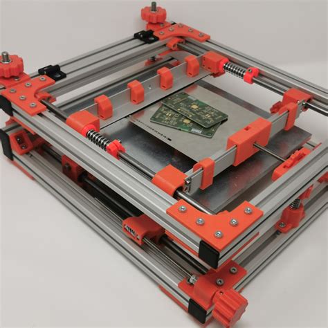
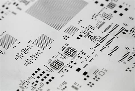
Printed Circuit Board (PCB) stencils are essential tools in the electronics manufacturing industry. They are thin, flat sheets of metal or plastic with precisely cut openings that correspond to the pads on a PCB. The stencil is used to apply solder paste onto the PCB pads before the components are placed and soldered. This process is known as solder paste printing or stencil printing.
PCB stencils ensure that the correct amount of solder paste is applied to each pad, resulting in a more reliable and consistent soldering process. They also help to reduce the amount of solder paste waste and improve the overall quality of the finished product.
Types of PCB Stencils
There are two main types of PCB stencils: metal stencils and plastic stencils.
- Metal Stencils:
- Made from stainless steel or nickel
- More durable and long-lasting
- Suitable for high-volume production
- Provide better paste release and print definition
-
More expensive than plastic stencils
-
Plastic Stencils:
- Made from polyester or other plastic materials
- More affordable than metal stencils
- Suitable for low-volume production or prototyping
- Less durable and may wear out faster
- Provide good paste release and print definition
PCB Stencil Thickness
The thickness of a PCB stencil is an important factor in determining the amount of solder paste deposited on the pads. The standard stencil thickness ranges from 0.1mm to 0.2mm (4-8 mils). Thicker stencils deposit more solder paste, while thinner stencils deposit less.
The optimal stencil thickness depends on various factors, such as the size and pitch of the components, the pad geometry, and the solder paste properties. It is essential to choose the right stencil thickness to ensure proper solder paste deposition and prevent issues like insufficient or excessive solder joints.
PCB Stencil Design Considerations
When designing a PCB stencil, several factors must be considered to ensure optimal performance and quality.
Aperture Size and Shape
The aperture size and shape of the stencil openings should match the size and shape of the PCB pads. The aperture size is typically slightly larger than the pad size to allow for proper solder paste deposition. The most common aperture shapes are rectangles and circles, but other shapes like ovals and diamonds may be used for specific applications.
Aperture Wall Angle
The aperture wall angle refers to the angle between the stencil surface and the aperture wall. A higher wall angle (closer to 90 degrees) provides better paste release and print definition but may be more challenging to manufacture. A lower wall angle (around 60 degrees) is easier to manufacture but may result in less precise prints.
Stencil Thickness and Aspect Ratio
The stencil thickness and aspect ratio (aperture width to stencil thickness) play a crucial role in determining the amount of solder paste deposited. A higher aspect ratio (larger aperture width relative to stencil thickness) allows for better paste release but may result in less precise prints. A lower aspect ratio provides better print definition but may lead to insufficient paste deposition.
Fiducial Marks and Alignment Features
Fiducial marks and alignment features are essential for accurate stencil alignment with the PCB. Fiducial marks are small, round, or cross-shaped features placed on the stencil and PCB to serve as reference points for alignment. Alignment features, such as pins or holes, help to physically align the stencil with the PCB during the printing process.

Solder Paste Printing Process
The solder paste printing process involves several steps to ensure proper solder paste deposition on the PCB pads.
- Stencil Alignment:
- The PCB is placed on the printer bed, and the stencil is aligned with the PCB using the fiducial marks and alignment features.
-
Proper alignment is crucial for accurate solder paste deposition.
-
Solder Paste Application:
- Solder paste is placed on the stencil surface, typically at one end of the stencil.
- A squeegee blade is used to spread the solder paste across the stencil surface, forcing it through the apertures and onto the PCB pads.
-
The squeegee pressure, speed, and angle are adjusted to achieve optimal solder paste deposition.
-
Stencil Removal:
- After the solder paste is applied, the stencil is carefully lifted away from the PCB.
-
The solder paste should release cleanly from the stencil apertures and remain on the PCB pads.
-
Inspection and Cleaning:
- The PCB is inspected to ensure that the solder paste is properly deposited on the pads and that there are no defects like bridging or insufficient paste.
- The stencil is cleaned to remove any residual solder paste and prepare it for the next printing cycle.

Stencil Cleaning and Maintenance
Proper stencil cleaning and maintenance are essential for ensuring consistent and high-quality solder paste printing.
Cleaning Methods
- Manual Cleaning:
- Using solvents and wiping materials to manually clean the stencil
- Suitable for small-scale production or quick cleaning between prints
-
Less thorough than automated cleaning methods
-
Automated Cleaning:
- Using specialized stencil cleaning machines with ultrasonic tanks, spray nozzles, and drying systems
- Provides more thorough and consistent cleaning
- Suitable for high-volume production and heavily contaminated stencils
Maintenance Practices
- Regular Inspection:
- Inspecting the stencil for signs of wear, damage, or contamination
-
Checking the aperture walls for any signs of clogging or damage
-
Proper Storage:
- Storing the stencil in a clean, dry environment to prevent contamination and damage
-
Using protective covers or cases to shield the stencil from dust and debris
-
Timely Replacement:
- Replacing the stencil when it shows signs of excessive wear or damage
- Using new stencils for critical applications or high-volume production

Frequently Asked Questions (FAQ)
- What is the difference between a metal and plastic PCB stencil?
-
Metal stencils are more durable, long-lasting, and suitable for high-volume production. They provide better paste release and print definition but are more expensive. Plastic stencils are more affordable, suitable for low-volume production or prototyping, but are less durable and may wear out faster.
-
How do I choose the right stencil thickness for my PCB?
-
The optimal stencil thickness depends on factors such as component size and pitch, pad geometry, and solder paste properties. Standard stencil thicknesses range from 0.1mm to 0.2mm (4-8 mils). Consult with your PCB manufacturer or stencil supplier to determine the best thickness for your specific application.
-
What are fiducial marks, and why are they important in PCB stencil design?
-
Fiducial marks are small, round, or cross-shaped features placed on the stencil and PCB to serve as reference points for alignment. They ensure accurate stencil alignment with the PCB during the solder paste printing process, resulting in precise solder paste deposition.
-
How often should I clean my PCB stencil?
-
The frequency of stencil cleaning depends on factors such as production volume, solder paste type, and environmental conditions. In general, it is recommended to clean the stencil after every print cycle or whenever there are signs of contamination or defects in the printed solder paste.
-
Can I reuse a damaged or worn-out PCB stencil?
- It is not recommended to reuse a damaged or worn-out PCB stencil, as it can lead to poor print quality, inconsistent solder paste deposition, and defects in the finished product. Replace the stencil when it shows signs of excessive wear or damage to ensure the best results.
Conclusion
PCB stencils are critical components in the electronics manufacturing process, ensuring accurate and consistent solder paste deposition on PCB pads. By understanding the types of stencils, design considerations, and the solder paste printing process, manufacturers can optimize their PCB assembly and achieve higher quality results.
Proper stencil cleaning and maintenance practices are equally important for maintaining consistent print quality and extending the stencil’s lifespan. Regular inspection, cleaning, and timely replacement of worn-out stencils are essential for ensuring reliable and efficient PCB production.
As PCB designs continue to evolve with smaller components and finer pitches, the importance of PCB stencils will only grow. Keeping up with the latest advancements in stencil technology and best practices will be crucial for manufacturers to stay competitive and meet the ever-increasing demands of the electronics industry.

No responses yet