Introduction to Solder Paste in SMT Assembly
Solder paste is a crucial component in the surface mount technology (SMT) assembly process for printed circuit boards (PCBs). It is a homogeneous mixture of tiny solder particles suspended in a flux medium, which helps to establish electrical and mechanical connections between surface mount components and the PCB. Solder paste printing is the process of applying this paste onto the PCB pads before component placement.
Composition of Solder Paste
Solder paste typically consists of the following components:
- Solder alloy particles (e.g., tin-lead, lead-free)
- Flux medium (e.g., rosin-based, water-soluble, no-clean)
- Additives (e.g., thickeners, stabilizers, rheology modifiers)
The solder alloy particles make up about 50-90% of the paste by weight, while the flux medium and additives account for the remaining portion.
Properties of Solder Paste
Solder paste has several essential properties that affect its performance in the SMT assembly process:
-
Particle size distribution: The size and distribution of solder particles impact the printing process, solder joint formation, and reliability.
-
Viscosity: The paste’s resistance to flow determines its printability and ability to maintain its shape after printing.
-
Slump resistance: The paste’s ability to resist deformation and maintain its printed geometry during handling and reflow.
-
Tack strength: The ability of the paste to hold components in place before reflow soldering.
-
Flux activity: The effectiveness of the flux in removing oxides and promoting solder wetting during reflow.
Solder Paste Printing Process
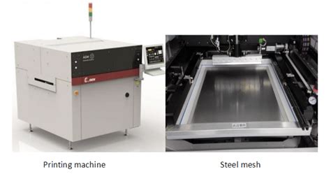
Stencil Design and Fabrication
Stencils are thin metal sheets (usually stainless steel or nickel) with apertures that match the PCB pad layout. They are used to transfer solder paste onto the PCB pads. Stencil design factors include:
- Aperture size and shape
- Stencil thickness
- Aperture wall smoothness and taper
- Fiducial marks for alignment
Stencils can be fabricated using various methods, such as laser cutting, electroforming, or etching.
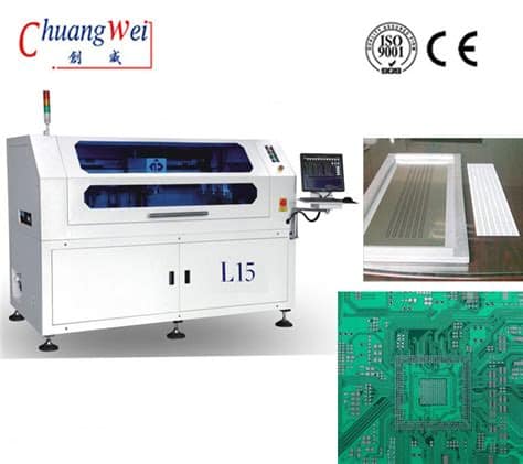
Solder Paste Printing Equipment
Solder paste printing is typically performed using automated stencil printers, which consist of the following components:
- Stencil frame and mounting system
- PCB support and clamping mechanism
- Paste dispensing system (e.g., squeegee blade, pump)
- Vision system for alignment and inspection
- Control software and user interface
Printing Process Steps
The solder paste printing process involves the following steps:
-
Stencil and PCB alignment: The stencil and PCB are aligned using fiducial marks and the printer’s vision system.
-
Solder paste application: The paste is dispensed onto the stencil surface, typically using an automated dispensing system.
-
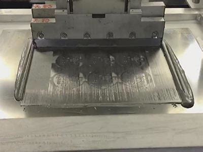
Squeegee blade printing: A squeegee blade is used to spread the paste across the stencil apertures, forcing it onto the PCB pads.
-
Stencil separation: The stencil is carefully lifted away from the PCB, leaving the printed solder paste deposits on the pads.
-
Inspection and touch-up: The printed PCB is inspected for defects, such as bridging, insufficient or excessive paste, or misalignment. Manual touch-up may be performed if necessary.
Printing Process Control and Optimization
To ensure consistent and reliable solder paste printing, several process parameters must be controlled and optimized:
-
Squeegee pressure and speed: Affects paste transfer efficiency and print definition.
-
Separation speed: Influences paste release from the stencil apertures and the shape of the printed deposits.
-
Print direction and pattern: Determines the sequence and orientation of the squeegee blade strokes.
-
Stencil cleaning: Regular cleaning is necessary to prevent paste buildup and maintain print quality.
-
Environmental control: Temperature, humidity, and cleanliness of the printing environment impact paste rheology and print performance.
Solder Paste Inspection and Defect Analysis
Solder Paste Inspection Methods
Solder paste inspection (SPI) is performed to verify the quality of the printed deposits before component placement. Common SPI methods include:
-
2D visual inspection: Uses machine vision to assess paste presence, alignment, and size in two dimensions.
-
3D measurement: Employs laser scanning or structured light techniques to measure paste volume, height, and shape in three dimensions.
-
X-ray inspection: Utilizes X-ray imaging to detect voids, foreign materials, or other internal defects in the paste deposits.
Common Solder Paste Printing Defects
Several defects can occur during solder paste printing, which may lead to assembly failures or reliability issues:
-
Insufficient or excessive paste: Results in poor solder joints or bridging.
-
Bridging or slumping: Occurs when paste spreads or collapses, causing short circuits between adjacent pads.
-
Misalignment or offsets: Happens when the printed deposits are not properly aligned with the PCB pads.
-
Stencil aperture clogging: Caused by paste buildup in the stencil apertures, leading to inconsistent or incomplete printing.
-
Scooping or dog-ears: Characterized by concave or raised edges on the printed deposits, often due to improper stencil separation.
Defect Analysis and Corrective Actions
When solder paste printing defects are identified, it is essential to analyze the root causes and implement corrective actions to prevent their recurrence. This may involve:
- Adjusting printing process parameters
- Modifying stencil design or fabrication
- Improving paste storage and handling practices
- Enhancing printer maintenance and calibration
- Providing operator training and guidance

Best Practices for Solder Paste Printing
To achieve optimal solder paste printing results and minimize defects, consider the following best practices:
-
Select appropriate paste and stencil specifications: Choose the paste and stencil that best suit your PCB Design, component types, and process requirements.
-
Control paste storage and handling: Ensure proper storage conditions (temperature, humidity) and follow manufacturer guidelines for paste shelf life and handling.
-
Implement robust printer setup and calibration: Regularly calibrate and maintain the printer to ensure accurate and consistent performance.
-
Optimize printing parameters: Conduct process characterization studies to determine the optimal settings for squeegee pressure, speed, separation, and other parameters.
-
Perform regular SPI and process monitoring: Use SPI systems to monitor print quality and identify trends or anomalies that may indicate process drift or impending failures.
-
Establish clear work instructions and training: Provide detailed, visual work instructions and training for operators to ensure consistent and correct execution of the printing process.
-
Foster continuous improvement: Regularly review process data, defect rates, and yields to identify opportunities for improvement and implement data-driven changes.
Frequently Asked Questions (FAQ)
-
What is the difference between solder paste and solder wire?
Solder paste is a mixture of solder particles and flux, used for SMT assembly, while solder wire is a solid wire of solder alloy, used for through-hole soldering and rework. -
How long can solder paste be stored, and what are the storage requirements?
Solder paste shelf life depends on the specific product and storage conditions. Generally, paste can be stored for 3-6 months at a controlled room temperature (20-25°C) and humidity (30-50% RH). Always refer to the manufacturer’s guidelines for storage and handling. -
What factors determine the choice of solder paste for a particular application?
When selecting a solder paste, consider factors such as the solder alloy composition, particle size, flux type, viscosity, and printing and reflow process requirements. The paste should be compatible with the PCB Surface Finish, component metallization, and the desired solder joint characteristics. -
How often should solder paste printing stencils be cleaned, and what cleaning methods are recommended?
Stencil cleaning frequency depends on the paste type, printing volume, and process conditions. Generally, stencils should be cleaned every 1-4 hours of continuous printing or between shifts. Common cleaning methods include manual wiping with solvents, ultrasonic cleaning, and automated understencil wiping systems. -
What are the key considerations when designing a solder paste printing stencil?
When designing a solder paste printing stencil, consider factors such as aperture size and shape, stencil thickness, aperture wall quality, and fiducial mark placement. The stencil design should be optimized for the specific PCB Layout, component types, and paste characteristics to ensure reliable and consistent printing results.
Conclusion
Solder paste printing is a critical process in SMT assembly that directly impacts the quality and reliability of solder joints. By understanding the characteristics of solder paste, the printing process steps, and the common defects and their causes, manufacturers can optimize their printing operations and achieve high yields and product quality. Implementing best practices, such as proper paste handling, printer maintenance, and process monitoring, can help to ensure consistent and reliable solder paste printing performance.
No responses yet