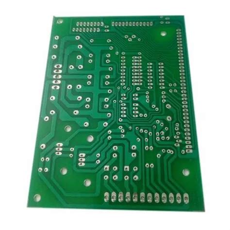
How Single-Sided PCBs are Manufactured
Single-sided PCBs are manufactured using a process called subtractive manufacturing. The process involves the following steps:
-
Substrate Preparation: A substrate, typically made of fiberglass or epoxy, is cut to the desired size and shape.
-
Copper Lamination: A thin layer of copper foil is laminated onto one side of the substrate using heat and pressure.
-
Artwork Application: The PCB design artwork is applied to the copper layer using a photoresist coating and exposure to UV light.
-
Etching: The exposed copper is etched away using a chemical solution, leaving only the desired conductive traces.
-
Drilling: Holes are drilled through the board for component mounting and vias, if required.
-
Finishing: The board is cleaned, and a solder mask is applied to protect the copper traces. Silkscreen printing may be added for component labels and other markings.
Advantages of Single-Sided PCBs
Single-sided PCBs offer several advantages, making them a popular choice for certain applications:
-
Cost-effectiveness: Single-sided PCBs are the most affordable option due to their simple manufacturing process and minimal material requirements.
-
Faster production: The manufacturing process for single-sided PCBs is relatively quick, allowing for shorter lead times.
-
Ease of design: Designing single-sided PCBs is simpler compared to more complex multi-layer boards, as there are fewer design considerations and constraints.
-
Reliability: Single-sided PCBs are suitable for low-density designs and can provide reliable performance for basic electronic projects.

Limitations of Single-Sided PCBs
While single-sided PCBs have their advantages, they also come with some limitations:
-
Limited routing options: With only one conductive layer, routing options are limited, which can lead to larger board sizes and increased wire jumpers.
-
Lower component density: Single-sided PCBs cannot accommodate high-density designs due to the limited space for components and traces.
-
Reduced electrical performance: The lack of a ground plane on single-sided PCBs can result in reduced electrical performance, particularly for high-frequency designs.
-
Limited heat dissipation: Single-sided PCBs have limited options for heat dissipation, which can be a concern for power-hungry components.

Applications of Single-Sided PCBs
Single-sided PCBs are widely used in various applications, particularly those with simple circuitry and low-density requirements. Some common applications include:
-
Consumer electronics: Simple devices such as calculators, toys, and remote controls often utilize single-sided PCBs.
-
Prototyping: Single-sided PCBs are often used for prototyping and proof-of-concept designs due to their quick turnaround times and low costs.
-
Educational purposes: Single-sided PCBs are ideal for educational projects and learning about PCB design and manufacturing processes.
-
Low-power applications: Devices with low power requirements, such as LED lighting and simple sensors, can often be implemented using single-sided PCBs.

Comparing Single-Sided PCBs with Other PCB Types
To better understand the role of single-sided PCBs, it’s essential to compare them with other common PCB types:
| PCB Type | Layers | Complexity | Cost | Applications |
|---|---|---|---|---|
| Single-sided | 1 | Low | Low | Simple designs, prototyping |
| Double-sided | 2 | Medium | Medium | More complex designs, improved routing |
| Multi-layer | 3+ | High | High | High-density designs, advanced applications |
As the table illustrates, single-sided PCBs are the simplest and most cost-effective option, while double-sided and multi-layer PCBs offer increased complexity and capabilities at a higher cost.
Designing Single-Sided PCBs
When designing single-sided PCBs, there are several key considerations to keep in mind:
-
Component placement: Carefully plan component placement to minimize the need for wire jumpers and optimize trace routing.
-
Trace width and spacing: Ensure that trace widths and spacing meet the manufacturing capabilities and electrical requirements of your design.
-
Via placement: If vias are required, strategically place them to minimize the impact on component placement and trace routing.
-
Solder mask and silkscreen: Consider the use of solder mask and silkscreen to protect the board and improve readability for assembly and maintenance.
-
Design rules: Adhere to the design rules and guidelines provided by your PCB manufacturer to ensure successful fabrication.
Manufacturing Considerations for Single-Sided PCBs
When manufacturing single-sided PCBs, there are several factors to consider:
-
Material selection: Choose the appropriate substrate material based on the electrical, mechanical, and environmental requirements of your application.
-
Copper thickness: Select the appropriate copper thickness for your design, considering factors such as current carrying capacity and trace width.
-
Solder mask and silkscreen: Decide on the color and type of solder mask and silkscreen to be used, based on aesthetic and functional requirements.
-
Surface finish: Select the appropriate surface finish, such as HASL, lead-free HASL, or immersion gold, depending on the soldering process and environmental concerns.
-
Panelization: Consider panelizing your design to maximize manufacturing efficiency and minimize costs, particularly for high-volume production.
Future of Single-Sided PCBs
Despite the increasing complexity of modern electronic devices, single-sided PCBs continue to play a significant role in the electronics industry. As technology advances, single-sided PCBs are likely to remain a viable option for certain applications, particularly those with simple circuitry and low-density requirements.
Furthermore, advancements in manufacturing processes and materials may enable single-sided PCBs to be used in more demanding applications. For example, the use of high-temperature substrates and advanced surface finishes could extend the capabilities of single-sided PCBs in harsh environments.
Frequently Asked Questions (FAQ)
-
Q: Can single-sided PCBs have through-hole components?
A: Yes, single-sided PCBs can accommodate through-hole components. The component leads are inserted through drilled holes and soldered on the opposite side of the board. -
Q: Are single-sided PCBs suitable for high-frequency designs?
A: Single-sided PCBs are generally not recommended for high-frequency designs due to the lack of a ground plane and limited routing options. For high-frequency applications, double-sided or multi-layer PCBs are typically used. -
Q: Can single-sided PCBs be used for surface-mount components?
A: Yes, surface-mount components can be used on single-sided PCBs. However, the limited routing options and lack of a ground plane may restrict the component density and performance compared to double-sided or multi-layer PCBs. -
Q: How do I choose the right substrate material for my single-sided PCB?
A: The choice of substrate material depends on factors such as the electrical requirements, operating temperature, and environmental conditions of your application. Common substrate materials for single-sided PCBs include FR-4, CEM-1, and CEM-3. -
Q: Can single-sided PCBs be used for flexible electronics?
A: Single-sided PCBs can be manufactured on flexible substrates, such as polyimide or PET, to create flexible electronics. These flexible single-sided PCBs are commonly used in applications that require bendability or conformity to irregular shapes.
In conclusion, single-sided PCBs are a simple, cost-effective, and reliable solution for basic electronic projects and low-density designs. While they may have limitations compared to more complex PCB types, they continue to play a vital role in the electronics industry and are likely to remain relevant in the future.
No responses yet