Understanding Silkscreen in PCB Manufacturing
Printed Circuit Boards (PCBs) are essential components in modern electronics, forming the backbone of devices we use every day. One crucial aspect of PCB design and manufacturing is the silkscreen layer. Silkscreen, also known as legend or nomenclature, is a printed layer on the PCB THAt provides valuable information for assembly, testing, and maintenance. In this article, we will dive deep into the world of silkscreen on PCBs, exploring its purpose, application methods, design considerations, and best practices.
What is Silkscreen?
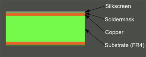
Silkscreen is a text and graphics layer printed on the surface of a PCB. It is typically white in color and contrasts with the PCB’s Solder Mask, making it easily readable. The silkscreen layer serves several purposes:
- Component identification: Silkscreen labels components with their reference designators (e.g., R1, C2, U3) and values (e.g., 10K, 100nF, 74HC00).
- Orientation markers: Silkscreen indicates the orientation of components, such as the polarity of diodes, electrolytic capacitors, and pin 1 of integrated circuits.
- Test points and fiducials: Silkscreen marks test points and fiducials, which are used for testing and automated assembly.
- Branding and information: Silkscreen can include company logos, product names, version numbers, and other relevant information.
Silkscreen Application Methods
There are two primary methods for applying silkscreen to PCBs:
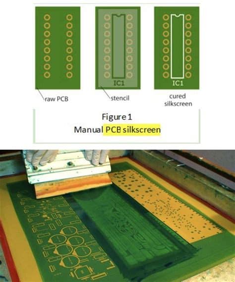
- Traditional silkscreen printing:
- A fine mesh screen is stretched over a frame, and the desired silkscreen pattern is created on the screen using a photo-reactive emulsion.
- Ink is then forced through the mesh onto the PCB surface using a squeegee.
-
This method is suitable for low-volume production and prototyping.
-
Direct legend printing:
- Silkscreen is directly printed onto the PCB using inkjet or laser printing technology.
- This method is faster and more precise than traditional silkscreen printing.
- Direct legend printing is ideal for high-volume production and offers greater design flexibility.
| Method | Advantages | Disadvantages |
|---|---|---|
| Traditional silkscreen printing | – Suitable for low-volume production – Cost-effective for small batches |
– Slower process – Limited design flexibility |
| Direct legend printing | – Fast and precise – Greater design flexibility – Ideal for high-volume production |
– Higher initial setup costs |
Silkscreen Design Considerations
When designing the silkscreen layer for your PCB, keep the following considerations in mind:
- Font size and style:
- Use a clear, legible font that is easy to read at small sizes (typically 0.8mm to 1.5mm in height).
-
Sans-serif fonts, such as Arial or Helvetica, are recommended for their readability.
-
Character spacing:
- Ensure adequate spacing between characters and lines to maintain legibility.
-
A minimum spacing of 0.15mm between characters and 0.3mm between lines is recommended.
-
Placement:
- Position silkscreen labels and markers to avoid obscuring component pads and traces.
-
Maintain a minimum clearance of 0.2mm between silkscreen and copper features.
-
Orientation:
- Orient text and graphics to be easily readable when the PCB is assembled and installed in its final application.
-
Consider the viewing angle and any obstructions that may hinder readability.
-
Contrast:
- Ensure sufficient contrast between the silkscreen and the solder mask to maintain legibility.
- White silkscreen on a dark solder mask (e.g., green, blue, black) provides the best contrast.
Best Practices for Silkscreen Design
To ensure optimal silkscreen quality and functionality, follow these best practices:
- Use vector graphics:
- Create silkscreen artwork using vector-based graphics software, such as Adobe Illustrator or Inkscape.
-
Vector graphics ensure crisp, high-resolution output and maintain quality when scaled.
-
Avoid unnecessary information:
- Include only essential information on the silkscreen layer to maintain clarity and reduce clutter.
-
Omit component values that are subject to change or are not critical for assembly or maintenance.
-
Consistent nomenclature:
- Use consistent and standardized naming conventions for component reference designators and labels.
-
Follow industry standards, such as IPC-7351B, for land pattern naming and component identification.
-
Verify silkscreen data:
- Double-check the accuracy of silkscreen information, including component references, values, and orientations.
-
Ensure that silkscreen data matches the schematic and Bill of Materials (BOM) to avoid assembly errors.
-
Consider manufacturing limitations:
- Consult with your PCB manufacturer to understand their silkscreen capabilities and limitations.
- Provide clear instructions and specifications for silkscreen application, including ink color, thickness, and any special requirements.
Frequently Asked Questions (FAQ)
-
Q: Can silkscreen be applied to both sides of a PCB?
A: Yes, silkscreen can be applied to both the top and bottom sides of a PCB, depending on the design requirements and assembly needs. -
Q: What is the minimum line width for silkscreen?
A: The minimum line width for silkscreen depends on the manufacturing process and the PCB fabricator’s capabilities. Typically, a minimum line width of 0.15mm to 0.2mm is achievable. -
Q: Can silkscreen be used for solder paste stencils?
A: No, silkscreen is not used for solder paste stencils. Solder paste stencils are typically made from laser-cut or chemically etched metal sheets, such as stainless steel or nickel. -
Q: Is it possible to have multiple colors of silkscreen on a PCB?
A: While it is technically possible to have multiple colors of silkscreen, it is not common practice. Most PCB designs use a single color (usually white) for simplicity and cost-effectiveness. -
Q: Can silkscreen be removed or modified after PCB manufacturing?
A: Silkscreen is a permanent part of the PCB and cannot be easily removed or modified after manufacturing. Any changes to the silkscreen require a new PCB production run.
Conclusion
Silkscreen is a vital component of PCB design and manufacturing, providing essential information for assembly, testing, and maintenance. By understanding the purpose, application methods, design considerations, and best practices associated with silkscreen, you can create PCBs that are clear, informative, and manufacturable. When designing your PCB’s silkscreen layer, prioritize legibility, clarity, and consistency to ensure a smooth and error-free manufacturing process. By following industry standards and collaborating with your PCB manufacturer, you can achieve high-quality silkscreen results that enhance the functionality and aesthetics of your PCB.

No responses yet