Introduction to Peelable Solder Mask
Peelable solder mask (PSM) is a specialized type of solder mask used in printed circuit board (PCB) manufacturing. Unlike traditional permanent solder masks, PSM can be easily removed or “peeled off” after the soldering process is complete. This unique property of peelable solder mask makes it a valuable tool for certain PCB Assembly applications and rework processes.
In this comprehensive article, we will dive deep into the world of peelable solder mask, exploring its composition, applications, advantages, and the process of using it in PCB manufacturing. We will also address some frequently asked questions about PSM to provide a complete understanding of this innovative material.
What is Solder Mask?
Before we delve into the specifics of peelable solder mask, let’s first understand what solder mask is and its role in PCB manufacturing.
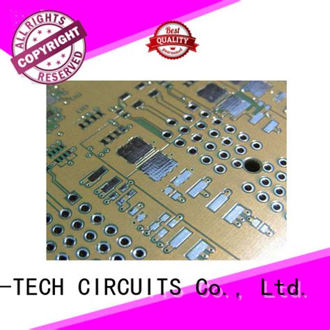
Solder mask, also known as solder resist or solder stop, is a thin layer of polymer applied to the copper traces of a PCB. Its primary purpose is to protect the copper from oxidation, prevent solder bridges from forming between closely spaced pads, and provide electrical insulation.
Solder mask is typically applied using screen printing or photoimaging techniques and is available in various colors, with green being the most common. The solder mask covers the entire PCB surface except for the areas where components will be soldered, such as pads and through-holes.

Composition of Peelable Solder Mask
Peelable solder mask is a specially formulated polymer designed to be easily removable after the soldering process. The exact composition of PSM varies between manufacturers but generally consists of the following components:
- Resin: The base material that provides the mask’s structural integrity and adhesion to the PCB surface.
- Fillers: Inorganic particles that improve the mask’s mechanical properties and control its viscosity.
- Additives: Various chemicals that enhance the mask’s performance, such as adhesion promoters, wetting agents, and defoamers.
- Pigments: Coloring agents that give the mask its distinctive color, typically blue or pink for easy identification.
The specific formulation of peelable solder mask is crucial to ensure that it adheres well to the PCB surface during the soldering process but can be easily peeled off without leaving residue or damaging the underlying circuitry.

Advantages of Peelable Solder Mask
Peelable solder mask offers several advantages over traditional permanent solder masks in specific PCB assembly and rework scenarios:
- Selective soldering: PSM allows for selective soldering of components, as the mask can be removed from specific areas without affecting the rest of the board.
- Rework and repair: When a component needs to be replaced or reworked, PSM can be easily peeled off, providing access to the pads and traces without damaging the PCB.
- Prototype and low-volume production: PSM is ideal for prototype and low-volume PCB assembly, as it eliminates the need for expensive solder mask stencils and allows for quick design iterations.
- Improved solderability: The removal of PSM after soldering can improve the solderability of the exposed pads and traces, as there is no risk of solder mask residue interfering with the solder joint formation.
- Cost-effective: For specific applications, using PSM can be more cost-effective than traditional solder masks, as it reduces the need for specialized equipment and simplifies the assembly process.

Applications of Peelable Solder Mask
Peelable solder mask finds use in various PCB assembly and rework applications, such as:
- BGA and QFN rework: PSM allows for easy access to the pads under Ball Grid Array (BGA) and Quad Flat No-lead (QFN) packages during rework, simplifying the component removal and replacement process.
- Selective conformal coating: By using PSM, specific areas of the PCB can be masked off during the conformal coating process, ensuring that critical components or connectors remain uncoated.
- Prototype and low-volume assembly: PSM is well-suited for prototype and low-volume PCB assembly, as it allows for quick design changes and eliminates the need for expensive solder mask stencils.
- High-density PCB assembly: The use of PSM can help prevent solder bridges and short circuits in high-density PCB designs, as the mask can be removed after soldering to expose the tightly spaced pads and traces.
- Selective soldering of through-hole components: PSM can be used to selectively solder through-hole components in mixed technology PCBs, where both surface mount and through-hole components are present.
The Process of Using Peelable Solder Mask
The process of using peelable solder mask in PCB manufacturing involves several steps:
- PCB design and fabrication: The PCB is designed and fabricated according to the desired specifications, with the copper traces and pads exposed.
- Peelable solder mask application: The PSM is applied to the PCB surface using screen printing or manual application methods. The mask covers the areas where soldering is not required.
- Soldering: The components are placed and soldered onto the PCB using standard soldering techniques, such as reflow or wave soldering.
- Peelable solder mask removal: After soldering, the PSM is carefully peeled off the PCB surface, exposing the soldered components and any areas that require further processing.
- Inspection and testing: The PCB is inspected for any solder defects or mask residue and undergoes necessary testing to ensure proper functionality.
It is essential to follow the manufacturer’s guidelines when using peelable solder mask, as factors such as application thickness, curing time, and removal technique can affect the mask’s performance and the overall quality of the PCB assembly.
Frequently Asked Questions (FAQ)
-
Q: Can peelable solder mask be used for all types of PCBs?
A: While PSM is versatile, it may not be suitable for all PCB designs. It is best suited for applications that require selective soldering, rework, or prototype assembly. High-volume production PCBs with intricate designs may be better served by traditional solder masks. -
Q: How does the cost of peelable solder mask compare to traditional solder masks?
A: The cost of PSM can vary depending on the specific formulation and manufacturer. In general, PSM may be more expensive per unit area than traditional solder masks. However, for specific applications, the overall cost savings from reduced equipment needs and simplified assembly processes can outweigh the higher material cost. -
Q: Can peelable solder mask be applied using automated methods?
A: Yes, PSM can be applied using automated screen printing equipment, similar to traditional solder masks. However, the specific viscosity and flow properties of PSM may require adjustments to the printing parameters to ensure optimal application. -
Q: Is peelable solder mask compatible with all soldering methods?
A: PSM is compatible with most common soldering methods, including reflow, wave, and hand soldering. However, it is essential to follow the manufacturer’s guidelines for temperature profiles and exposure times to ensure the mask’s integrity during the soldering process. -
Q: How do I ensure that peelable solder mask is completely removed after soldering?
A: To ensure complete removal of PSM, it is crucial to follow the manufacturer’s guidelines for peeling techniques and timing. Some tips include using tweezers or a sharp blade to start the peeling process, pulling the mask at a low angle to the PCB surface, and visually inspecting the board after removal to check for any residue. If necessary, gentle cleaning with isopropyl alcohol can help remove any remaining traces of PSM.
Conclusion
Peelable solder mask is a valuable tool in PCB manufacturing, offering unique advantages for selective soldering, rework, and prototype assembly applications. By understanding its composition, applications, and the process of using PSM, PCB designers and assembly engineers can leverage this innovative material to optimize their manufacturing processes and improve the overall quality of their products.
As the electronics industry continues to evolve, with ever-increasing demands for miniaturization and high-density PCB designs, peelable solder mask will likely play a growing role in enabling efficient and cost-effective manufacturing solutions.
Comparison of Solder Mask Types
| Solder Mask Type | Permanent | Peelable |
|---|---|---|
| Composition | Epoxy or acrylic-based polymers | Specially formulated polymers with removable properties |
| Application | Screen printing, photoimaging | Screen printing, manual application |
| Removal | Not designed for removal | Easily peeled off after soldering |
| Typical Uses | High-volume production, standard PCB designs | Selective soldering, rework, prototype assembly |
| Cost | Lower material cost, higher equipment investment | Higher material cost, lower equipment investment |
Peelable Solder Mask Application Steps
- PCB Design and Fabrication
- Peelable Solder Mask Application
- Soldering
- Peelable Solder Mask Removal
- Inspection and Testing
By carefully considering the specific requirements of their PCB assembly projects and leveraging the unique properties of peelable solder mask when appropriate, manufacturers can optimize their processes, reduce costs, and deliver high-quality products to their customers.
No responses yet