Introduction to PCB Vias
A Printed Circuit Board (PCB) is a fundamental component in modern electronics. It provides a platform for mounting and connecting various electronic components to form a functional circuit. One crucial aspect of PCB design is the use of vias, which play a vital role in interconnecting different layers of a multi-layer PCB. In this article, we will explore PCB vias in detail, including their types, applications, and manufacturing processes.
What are PCB Vias?
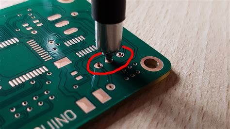
PCB vias are small holes drilled through a PCB to create electrical connections between different layers of the board. They allow signals and power to be routed from one layer to another, enabling more complex circuit designs and efficient use of board space. Vias are typically plated with a conductive material, such as copper, to ensure reliable electrical connections.
Types of PCB Vias
There are several types of PCB vias, each serving a specific purpose in PCB design. Let’s explore the most common types:
Through-Hole Vias
Through-hole vias are the most basic type of via. They are drilled completely through the PCB, from the top layer to the bottom layer. These vias are typically used for mounting through-hole components or for providing electrical connections between layers in simpler PCB designs.
Blind Vias
Blind vias are drilled from one side of the PCB and terminate at a specific inner layer, without reaching the opposite side of the board. They are used to connect an outer layer to one or more inner layers, allowing for more compact and efficient PCB designs.
Buried Vias
Buried vias are located entirely within the inner layers of a PCB and do not extend to either the top or bottom layer. They are used to interconnect inner layers without consuming space on the outer layers, enabling higher component density and more complex routing.
Micro Vias
Micro vias are small-diameter vias, typically less than 150 microns in diameter. They are used in high-density PCB designs to create fine-pitch interconnections between layers. Micro vias are often laser-drilled and are essential for advanced packaging technologies, such as chip-scale packages (CSPs) and ball grid arrays (BGAs).
Via Hole Size and Aspect Ratio
The size of a via hole is an important consideration in PCB design. The diameter of the hole depends on the intended purpose, the thickness of the PCB, and the manufacturing capabilities. Smaller via holes allow for denser routing and more compact designs, but they also pose challenges in manufacturing and reliability.
The aspect ratio of a via is the ratio of its depth to its diameter. A higher aspect ratio means a deeper and narrower via, which can be more difficult to manufacture and plate properly. PCB designers must consider the aspect ratio when selecting via sizes to ensure manufacturability and reliable electrical connections.

PCB Via Manufacturing Process
The manufacturing process for PCB vias involves several steps to ensure proper formation and reliable electrical connections. Let’s explore the key steps in via manufacturing:
Drilling
The first step in creating PCB vias is drilling holes through the PCB substrate. This is typically done using mechanical drilling machines or laser drilling systems, depending on the via size and type. Mechanical drilling is suitable for larger through-hole vias, while laser drilling is often used for smaller, high-density vias and micro vias.
Deburring and Cleaning
After drilling, the via holes must be deburred and cleaned to remove any debris or rough edges. Deburring ensures smooth hole walls and prevents issues during the plating process. Cleaning removes any contaminants that may affect the adhesion of the plating material.
Electroless Copper Deposition
The next step is to deposit a thin layer of copper onto the via hole walls using an electroless copper plating process. This process involves immersing the PCB in a chemical bath that contains a copper solution. The copper ions in the solution adhere to the hole walls, forming a thin, conductive layer that acts as a seed layer for subsequent plating.
Electrolytic Copper Plating
After the electroless copper deposition, the via holes undergo an electrolytic copper plating process. This involves applying an electric current to the PCB while it is immersed in a copper plating solution. The electric current causes the copper ions to deposit onto the seed layer, building up a thicker, more conductive layer of copper in the via holes.
Filling and Capping (Optional)
In some cases, via holes may be filled with a conductive or non-conductive material to improve reliability, prevent solder wicking, or provide additional mechanical support. Via filling is often done using a screen printing process or a specialized via filling machine. After filling, the vias may be capped with a copper layer to create a smooth surface for subsequent processing.

PCB Via Applications
PCB vias are used in a wide range of electronic applications, from simple single-layer boards to complex multi-layer designs. Some common applications include:
High-Density Interconnect (HDI) PCBs
HDI PCBs are designed with a high density of components and interconnections, often using micro vias and fine-pitch BGAs. These PCBs are used in advanced electronic devices, such as smartphones, tablets, and wearables, where space is limited, and performance demands are high.
Multilayer PCBs
Multilayer PCBs consist of multiple layers of conductive material separated by insulating layers. Vias are used to interconnect these layers, allowing for more complex routing and higher component density. Multilayer PCBs are used in a wide range of applications, from consumer electronics to industrial control systems and aerospace equipment.
Power Electronics
In power electronic applications, such as switching power supplies and motor drives, PCB vias play a crucial role in providing low-impedance connections between power components and ground planes. Properly designed vias help minimize parasitic inductance and resistance, improving power efficiency and reducing electromagnetic interference (EMI).
RF and Microwave PCBs
PCB vias are critical in radio frequency (RF) and Microwave PCB Designs, where signal integrity and controlled impedance are essential. Vias in these applications must be carefully designed and placed to minimize signal reflections, crosstalk, and losses. Specialized via structures, such as coaxial vias and shielded vias, are often used in RF and microwave PCBs to maintain signal integrity.

PCB Via Design Considerations
When designing PCB vias, several factors must be considered to ensure optimal performance, reliability, and manufacturability. Some key considerations include:
Signal Integrity
Vias can introduce discontinuities in signal paths, leading to reflections, losses, and crosstalk. Designers must carefully consider via placement, size, and spacing to minimize these effects and maintain signal integrity. Techniques such as via shielding, ground vias, and differential pair routing can help mitigate signal integrity issues.
Thermal Management
Vias can also play a role in thermal management by providing a path for heat dissipation from components to other layers or heat sinks. Thermal vias, which are typically filled with a thermally conductive material, are used to transfer heat away from high-power components, improving reliability and preventing overheating.
Manufacturing Constraints
PCB via design must take into account the capabilities and limitations of the manufacturing process. Factors such as via hole size, aspect ratio, and spacing must be carefully considered to ensure manufacturability and reliability. Designers should work closely with PCB manufacturers to understand their specific design rules and constraints.
Cost and Complexity
The number and type of vias used in a PCB design can significantly impact the overall cost and complexity of the board. More complex via structures, such as blind and buried vias, require additional manufacturing steps and may increase the cost of the PCB. Designers must balance the need for advanced via technologies with cost and manufacturing considerations.
Frequently Asked Questions (FAQ)
- What is the difference between a through-hole via and a blind via?
-
A through-hole via extends through the entire thickness of the PCB, connecting the top and bottom layers. A blind via, on the other hand, starts from one surface of the PCB and terminates at an inner layer, without reaching the opposite surface.
-
What is the purpose of via filling?
-
Via filling is the process of filling via holes with a conductive or non-conductive material. It is done to improve reliability, prevent solder wicking, provide mechanical support, or create a smooth surface for subsequent processing steps.
-
How do vias affect signal integrity in high-speed PCBs?
-
Vias can introduce discontinuities in signal paths, leading to reflections, losses, and crosstalk. These effects become more pronounced at higher frequencies. Proper via design, placement, and techniques such as via shielding and ground vias can help mitigate signal integrity issues in high-speed PCBs.
-
What is the role of vias in thermal management?
-
Vias can provide a path for heat dissipation from components to other layers or heat sinks. Thermal vias, which are filled with a thermally conductive material, are used to transfer heat away from high-power components, improving reliability and preventing overheating.
-
How do manufacturing constraints affect via design?
- Manufacturing constraints, such as via hole size, aspect ratio, and spacing, must be considered when designing vias. These constraints are determined by the capabilities and limitations of the PCB manufacturing process. Designers should work closely with PCB manufacturers to ensure that their via designs are manufacturable and reliable.
Conclusion
PCB vias are essential components in modern PCB design, enabling the creation of complex, high-density, and multi-layer circuits. By understanding the types of vias, their manufacturing processes, applications, and design considerations, PCB designers can create reliable, high-performance electronic products that meet the demands of today’s technology landscape. As electronic devices continue to evolve and become more sophisticated, the role of PCB vias will remain crucial in enabling the next generation of innovative and efficient electronic solutions.
No responses yet