Why Use a PCB Stencil?
PCB stencils are essential for several reasons:
- Precision: Stencils ensure that the correct amount of solder paste is applied to each pad on the PCB, which is crucial for creating reliable solder joints.
- Consistency: Using a stencil guarantees that the solder paste is applied consistently across the entire PCB, reducing the risk of defects caused by uneven solder paste application.
- Efficiency: Stencils allow for the rapid application of solder paste to multiple PCBs, making the assembly process more efficient and cost-effective.
Types of PCB Stencils
There are two main types of PCB stencils:
1. Stainless Steel Stencils
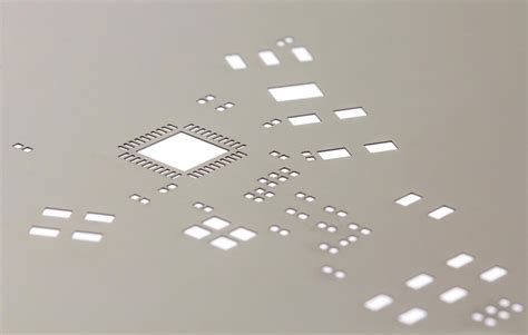
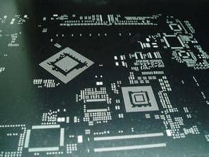
Stainless steel stencils are the most common type of PCB stencil. They are durable, long-lasting, and suitable for high-volume production. Stainless steel stencils are typically laser-cut or chemically etched to create the openings for solder paste application.
Advantages of Stainless Steel Stencils
- High durability and long lifespan
- Suitable for high-volume production
- Excellent paste release properties
- Low thermal expansion for better accuracy
Disadvantages of Stainless Steel Stencils
- Higher initial cost compared to polyimide stencils
- Less flexible than polyimide stencils
- Requires proper maintenance to prevent damage
2. Polyimide Stencils
Polyimide stencils, also known as polymer stencils, are made from a flexible, high-temperature resistant plastic material. They are typically used for prototyping, low-volume production, or when a more flexible stencil is required.
Advantages of Polyimide Stencils
- Lower cost compared to stainless steel stencils
- Flexibility allows for better conformity to uneven surfaces
- Suitable for prototyping and low-volume production
Disadvantages of Polyimide Stencils
- Lower durability compared to stainless steel stencils
- Not suitable for high-volume production
- Can be prone to stretching or tearing with repeated use

Stencil Thickness and Aperture Design
The thickness of a PCB stencil and the design of its apertures (openings) play a crucial role in determining the quality of solder paste application.
Stencil Thickness
Stencil thickness is typically measured in microns (μm) or mils (thousandths of an inch). The most common stencil thicknesses range from 100μm to 150μm (4-6 mils). Thicker stencils are used for larger components or when more solder paste is required, while thinner stencils are used for smaller components or finer pitch devices.
| Stencil Thickness | Typical Applications |
|---|---|
| 100μm (4 mils) | Fine pitch components, small chip components |
| 120μm (5 mils) | General-purpose, most common thickness |
| 150μm (6 mils) | Larger components, higher volume solder paste deposits |
Aperture Design
Aperture design refers to the shape, size, and orientation of the openings in the stencil. Properly designed apertures ensure that the correct amount of solder paste is deposited onto each pad and that the paste releases easily from the stencil.
Aperture Shapes
The most common aperture shapes are rectangular and circular. Rectangular apertures are used for most SMD pads, while circular apertures are used for round pads, such as those found on ball grid array (BGA) components.
Aperture Size
Aperture size is typically expressed as a percentage of the pad size. For example, a 1:1 ratio means that the aperture size is equal to the pad size. In general, aperture sizes range from 80% to 120% of the pad size, depending on the component type and desired solder volume.
| Aperture Size | Typical Applications |
|---|---|
| 80-90% | Fine pitch components, small chip components |
| 100% | General-purpose, most common size |
| 110-120% | Larger components, higher volume solder paste deposits |
Aperture Orientation
Aperture orientation refers to the alignment of the aperture with respect to the pad. In most cases, apertures are oriented to match the pad orientation. However, in some cases, such as with fine pitch components, apertures may be rotated slightly to improve paste release and prevent bridging.

Stencil Frame and Mounting
PCB stencils are typically mounted in a frame to ensure proper alignment with the PCB and to facilitate handling during the solder paste application process.
Stencil Frame Types
There are two main types of stencil frames:
- Aluminum Frames: Aluminum frames are the most common type of stencil frame. They are lightweight, durable, and provide good rigidity for the stencil.
- Magnetic Frames: Magnetic frames use magnets to hold the stencil in place. They allow for quick and easy stencil changes, making them ideal for high-mix, low-volume production.
Stencil Mounting Methods
There are several methods for mounting a stencil to its frame:
- Adhesive Mounting: The stencil is bonded to the frame using a high-strength adhesive. This method provides a secure, permanent bond but makes stencil replacement more difficult.
- Mechanical Mounting: The stencil is held in place using mechanical fasteners, such as screws or clamps. This method allows for easier stencil replacement but may not provide as secure a bond as adhesive mounting.
- Magnetic Mounting: The stencil is held in place using magnets, as with magnetic frames. This method allows for quick and easy stencil changes but may not be suitable for very fine pitch applications.

Stencil Cleaning and Maintenance
Proper cleaning and maintenance of PCB stencils are essential for ensuring consistent solder paste application and preventing defects.
Cleaning Frequency
Stencils should be cleaned regularly to remove any excess solder paste, debris, or contamination. The cleaning frequency depends on several factors, including:
- Production volume
- Solder paste type
- Environmental conditions
- Stencil material
As a general guideline, stencils should be cleaned every 4-8 hours of continuous use or between production shifts.
Cleaning Methods
There are two main methods for cleaning PCB stencils:
- Manual Cleaning: Manual cleaning involves using solvents and wiping materials to remove solder paste and debris from the stencil by hand. This method is suitable for low-volume production or when automated cleaning equipment is not available.
- Automated Cleaning: Automated cleaning uses specialized equipment, such as stencil cleaning machines, to clean the stencil. This method is more efficient and consistent than manual cleaning and is suitable for high-volume production.
Stencil Storage
When not in use, PCB stencils should be stored properly to prevent damage and contamination. Stencils should be stored in a clean, dry environment, away from direct sunlight and extreme temperatures. They should also be stored flat or hung vertically to prevent warping or deformation.
Frequently Asked Questions (FAQ)
1. What is the difference between a Solder paste stencil and a solder mask?
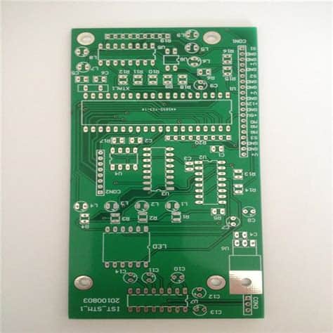
A solder paste stencil is used to apply solder paste to the pads on a PCB, while a solder mask is a protective layer applied to the PCB that prevents solder from adhering to unwanted areas. Solder paste stencils are used during the assembly process, while solder masks are part of the PCB fabrication process.
2. Can I use the same stencil for different PCB Designs?
In most cases, each PCB design requires its own unique stencil. This is because the stencil apertures must match the pad sizes and locations on the specific PCB. However, if you have multiple PCB designs with identical pad layouts, you may be able to use the same stencil for those designs.
3. How long do PCB stencils last?
The lifespan of a PCB stencil depends on several factors, including the stencil material, cleaning and maintenance practices, and production volume. Stainless steel stencils typically last longer than polyimide stencils. With proper care and maintenance, a stainless steel stencil can last for tens of thousands of prints, while a polyimide stencil may last for several thousand prints.
4. What is the best way to store PCB stencils when not in use?
PCB stencils should be stored in a clean, dry environment, away from direct sunlight and extreme temperatures. They should be stored flat or hung vertically to prevent warping or deformation. Stencils should also be protected from damage by storing them in dedicated stencil storage racks or containers.
5. How do I choose the right stencil thickness for my PCB?
The choice of stencil thickness depends on several factors, including the component sizes, pad sizes, and desired solder paste volume. As a general rule, thinner stencils (100-120μm) are used for smaller components and finer pitch devices, while thicker stencils (120-150μm) are used for larger components and higher volume solder paste deposits. It’s best to consult with your stencil supplier or assembly service provider to determine the optimal stencil thickness for your specific PCB design.

No responses yet