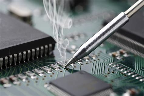
Introduction to PCB Assembly
PCB assembly is the process of populating a printed circuit board (PCB) with electronic components to create a functional circuit. It involves soldering components such as resistors, capacitors, and integrated circuits onto the board in the correct locations according to the PCB design.
PCB assembly is a critical step in electronics manufacturing. Most modern electronic devices, from smartphones to medical equipment, rely on PCBs to function. Proper PCB assembly ensures the reliability and performance of these devices.
In this comprehensive guide, we’ll cover everything beginners need to know about PCB assembly, including the types of PCB assembly, the process, tools and equipment needed, and best practices for achieving high-quality results.
Types of PCB Assembly
There are two main types of PCB assembly: through-hole and surface mount.
Through-Hole Assembly
Through-hole assembly involves inserting component leads through holes drilled in the PCB and soldering them to pads on the opposite side. This method is older and less common today, but is still used for some applications due to its durability and ease of repair.
Advantages of through-hole assembly include:
- Strong mechanical connections
- Easy to solder by hand
- Components can be replaced easily
Disadvantages include:
- Larger component size
- Drilling holes takes extra time and cost
- Not suitable for high-density designs
Surface Mount Assembly
Surface mount assembly has largely replaced through-hole in modern electronics manufacturing. With this method, components are soldered directly onto pads on the surface of the PCB without going through holes.
Surface mount components are much smaller than through-hole components, allowing for denser PCB designs. The lack of drilled holes also reduces manufacturing time and cost.
Advantages of surface mount assembly include:
- Smaller component size
- Higher component density possible
- Faster and cheaper assembly
- Better high-frequency performance
Disadvantages include:
- Components are harder to solder by hand
- Requires specialized equipment for assembly
- More difficult to repair or replace components

The PCB Assembly Process
The PCB assembly process typically involves the following steps:
-
Solder Paste Application – A thin layer of solder paste is applied to the PCB pads using a stencil. Solder paste is a mixture of tiny solder balls suspended in flux.
-
Component Placement – A pick-and-place machine or by hand, components are positioned on the PCB pads. The stickiness of the solder paste holds components in place.
-
Reflow Soldering – The populated PCB is run through a reflow oven. The solder paste melts, forming a permanent solder joint between component leads and PCB pads as it cools.
-
Inspection and Test – The assembled PCB is visually inspected and electrically tested to ensure proper functionality before moving on to final assembly into the end product.
Here’s a table summarizing the key steps:
| Step | Description |
|---|---|
| Solder Paste Application | Apply solder paste to PCB pads |
| Component Placement | Place components on solder paste |
| Reflow Soldering | Melt solder paste to form joints |
| Inspection and Test | Check for defects and functionality |
The exact process can vary depending on the specific PCB design, components used, and production volume. High volume PCB assembly often uses automated equipment to optimize speed and consistency.

PCB Assembly Equipment
The equipment needed for PCB assembly depends on the type of assembly (through-hole vs surface mount) and production volume. Key pieces of equipment include:
Soldering Iron
For manual soldering of through-hole components. A basic soldering iron for electronics work should have adjustable temperature control and interchangeable tips.
Reflow Oven
Used for surface mount assembly to melt the solder paste and form solder joints. Reflow ovens have a controlled heating profile to gradually raise the temperature of the PCB and components.
Pick-and-Place Machine
Automated machine that picks up surface mount components and places them in the correct position on the PCB. Essential for high volume production.
Stencil Printer
Used to apply solder paste to the PCB pads through a laser-cut stencil. Ensures an even layer of paste is applied in the correct locations.
Inspection Microscope
Allows close visual inspection of solder joints and components for defects. A microscope with built-in LED lighting and adjustable zoom is recommended.
Here’s a table of common PCB assembly equipment:
| Equipment | Description |
|---|---|
| Soldering Iron | Manual soldering of through-hole components |
| Reflow Oven | Melts solder paste for surface mount assembly |
| Pick-and-Place Machine | Automated component placement |
| Stencil Printer | Applies solder paste to PCB pads |
| Inspection Microscope | Close visual inspection of solder joints |
The specific equipment needed will depend on the PCB assembler’s setup and the types of PCBs being assembled. Investing in high-quality equipment is important for producing reliable PCB assemblies.

PCB Assembly Best Practices
Following best practices during PCB assembly can help ensure a high-quality, reliable end product. Some key best practices include:
Use the Right Solder
Use solder that is appropriate for the components and PCB finish. Lead-free solder is now standard for most commercial electronics. Solder wire should have a rosin core to help the solder flow and adhere properly.
Keep Things Clean
PCBs and components should be clean and free of dirt, grease, and oxidation before assembly. Isopropyl alcohol can be used to clean PCBs. Gloves should be worn to avoid contaminating surfaces with skin oils.
Control Soldering Temperature
Use the correct soldering iron tip temperature for the solder type. Too high of a temperature can damage components or lift PCB pads. Too low of a temperature will result in poor solder joints.
Inspect Solder Joints
Visually inspect solder joints for defects such as bridging (solder connecting adjacent pins), insufficient solder, or voids in the joint. X-ray inspection may be needed for joints under chips.
Use ESD Protection
Electronic components can be damaged by electrostatic discharge (ESD). Wear an ESD wrist strap when handling PCBs and components. Use an ESD-safe mat on the work surface.
Here’s a table summarizing some key best practices:
| Best Practice | Importance |
|---|---|
| Use Correct Solder | Ensure proper solder joint formation |
| Keep Things Clean | Avoid contamination that can affect soldering |
| Control Soldering Temperature | Prevent component and PCB damage |
| Inspect Solder Joints | Catch any soldering defects early |
| Use ESD Protection | Prevent damage to sensitive components |
Following these best practices can help produce high-quality PCB assemblies with fewer defects and failures in the field. Many of these practices become standard procedure in a professional PCB assembly environment.
Common PCB Assembly Defects
Even with proper procedures and equipment, PCB assembly defects can still occur. Some common types of defects include:
Bridging
This is when solder inadvertently connects two adjacent pins or pads that should not be connected. Bridging is more common with fine-pitch surface mount components.
Tombstoning
This occurs when one end of a surface mount component stands up vertically on the PCB instead of lying flat. It is caused by uneven heating or an imbalance in solder paste volume on the component pads.
Insufficient solder
Also known as a “dry joint”, this is when not enough solder is applied to a joint, resulting in a weak connection. It can be caused by too little solder paste being applied or the soldering temperature being too low.
Solder balls
These are small spheres of solder that are not part of a proper joint. They can occur due to excessive solder paste or improper reflow oven settings. Solder balls can cause short circuits if they land between pins.
Here’s a table of these common defects and their causes:
| Defect | Cause |
|---|---|
| Bridging | Solder connecting adjacent pins/pads |
| Tombstoning | Uneven component heating or solder volume |
| Insufficient Solder | Too little solder applied to joint |
| Solder Balls | Excess solder or improper reflow settings |
Most of these defects can be prevented with proper process control, but some level of defects is still common. Defects should be identified and repaired during post-assembly inspection to ensure the reliability of the final product.
PCB Assembly Services
Many electronics companies outsource their PCB assembly to specialized PCB assembly services instead of doing it in-house. Using a PCB assembly service offers several advantages:
Expertise
PCB assembly services have the specialized skills and experience to assemble a wide variety of PCBs reliably and efficiently. They are familiar with the latest components and assembly techniques.
Equipment
Assembling PCBs, especially with surface mount components, requires expensive equipment like pick-and-place machines, reflow ovens, and inspection systems. PCB assembly services already have this equipment in place.
Scalability
PCB assembly services can handle both small prototype runs and large volume production. They can scale up assembly as needed to meet demand.
Cost savings
Outsourcing PCB assembly avoids the need to invest in equipment and train staff. It can be more cost-effective than setting up an in-house assembly line, especially for lower production volumes.
When selecting a PCB assembly service, consider factors such as:
- Experience with similar PCB designs
- Quality certifications such as ISO 9001
- Turnaround time and pricing
- Ability to source components
- Prototyping and testing services offered
Many PCB assembly services offer online quoting and ordering to streamline the process. They typically work from the OEM’s PCB design files, bill of materials (BOM), and assembly drawings.
FAQ
What is a PCB?
A: A PCB, or printed circuit board, is a flat board made of insulating material with conductive copper traces on one or both sides. It mechanically supports and electrically connects electronic components using the conductive pathways.
What are the types of PCB assembly?
A: The two main types of PCB assembly are through-hole assembly and surface mount assembly. Through-hole involves inserting component leads through holes in the PCB, while surface mount solders components directly to pads on the PCB surface.
What equipment is needed for PCB assembly?
A: Key equipment for PCB assembly can include soldering irons, reflow ovens, pick-and-place machines, stencil printers, and inspection microscopes. The specific equipment depends on the type of assembly and production volume.
What are some common PCB assembly defects?
A: Common PCB assembly defects include bridging (solder connecting adjacent pins/pads), tombstoning (one end of a component lifting up), insufficient solder in a joint, and solder balls that can cause short circuits.
Why use a PCB assembly service?
A: PCB assembly services offer expertise, specialized equipment, scalability, and potential cost savings compared to in-house assembly. They can handle a range of PCB types and production volumes.
No responses yet