Introduction to NB2DSK01 SPI Flash
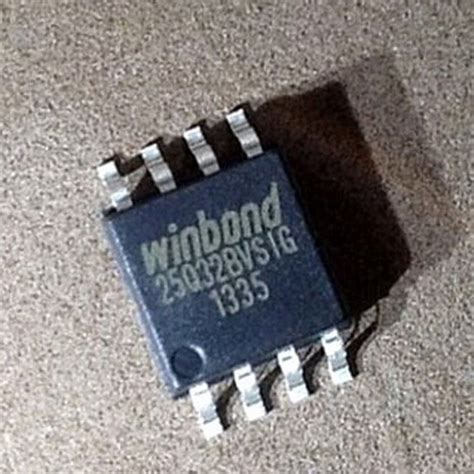
The NB2DSK01 is a type of serial SPI flash memory device. It provides non-volatile storage that retains data even when power is removed. This makes it useful for storing firmware, configuration settings, and other persistent data in embedded systems and electronics projects.
Key Features of NB2DSK01 Flash
Some of the key characteristics and benefits of the NB2DSK01 SPI flash include:
- High storage density in a small package
- Fast SPI interface with speeds up to 104 MHz
- Low power consumption
- Flexible erase and programming options
- Built-in features for security and reliability
The table below summarizes the key specifications of the NB2DSK01:
| Parameter | Value |
|---|---|
| Density | 1 Mb – 2 Mb |
| Voltage | 2.7V – 3.6V |
| Max SPI Clock | 104 MHz |
| Packaging | 8-pin SOP, 8-contact WSON |
| Temperature | -40°C to +85°C |
Advantages of Serial NOR Flash like NB2DSK01
NOR flash memory like the NB2DSK01 has several advantages compared to other non-volatile memory technologies:
-
Byte-addressable: NOR flash allows direct access and execution of code stored in the memory. This enables storing firmware that can run directly from the flash (execute-in-place or XIP).
-
High reliability: NOR flash is known for high endurance and data retention. Stored data remains intact for many years and the flash can withstand a large number of erase/program cycles.
-
Fast random access: The memory array can be accessed randomly with low latency, similar to RAM. This suits storing code and data structures that are frequently accessed in a non-linear fashion.
-
Ease of use: NOR flash connects easily to microcontrollers and processors over the simple SPI interface. Standard command sets allow interoperability between different vendors.
NB2DSK01 Memory Organization and Operation
NB2DSK01 Density Options and Memory Map
The NB2DSK01 flash is available in two density options:
- 1 Mb (128 KB) organized as 131,072 bytes
- 2 Mb (256 KB) organized as 262,144 bytes
The memory is arranged in 4 KB sectors and 64 KB blocks. Each sector can be individually erased. The entire memory can be erased in a bulk operation.
The memory map of the 1 Mb NB2DSK01 looks like:
| Address Range | Contents |
|---|---|
| 0x1F000-0x1FFFF | 4 KB Sector 31 |
| 0x1E000-0x1EFFF | 4 KB Sector 30 |
| … | … |
| 0x01000-0x01FFF | 4 KB Sector 1 |
| 0x00000-0x00FFF | 4 KB Sector 0 |
The 2 Mb version has double the number of sectors.
Connecting NB2DSK01 to an MCU over SPI
The NB2DSK01 uses a 4-wire SPI interface to communicate with a host controller. The interface signals are:
- CS#: Chip Select (active low)
- CLK: Serial Clock (up to 104 MHz)
- SI: Serial Input (data from host to flash)
- SO: Serial Output (data from flash to host)
To connect the NB2DSK01 to a microcontroller SPI peripheral:
- Connect CS# to an MCU GPIO pin configured as chip select
- Connect CLK to the MCU SPI clock output
- Connect SI to the MCU SPI MOSI output
- Connect SO to the MCU SPI MISO input
- Pull up CS#, hold RESET# high, connect power and ground
Here is an example connection diagram:
   MCU                 NB2DSK01
+-------+             +---------+
|     CS|-------------|CS#      |
|    CLK|-------------|CLK      |
|   MOSI|-------------|SI       |
|   MISO|-------------|SO       |
|     VCC---|   |----|VCC     |
|     GND---|   |----|GND     |
+-------+    |   |    +---------+
             |   |----|RESET#
             +---|----| WP#
NB2DSK01 Instruction Set and Basic Operations
The NB2DSK01 utilizes a standard set of SPI flash instructions to perform operations like reading, writing and erasing. Each instruction consists of an 8-bit opcode followed by any required address and data bytes.
Here are some of the key instructions:
| Instruction | Opcode | Description |
|---|---|---|
| READ | 0x03 | Read data bytes from memory |
| FAST_READ | 0x0B | Read data bytes at higher speed |
| PP | 0x02 | Program (write) data into memory |
| SE | 0x20 | Erase a 4KB sector |
| BE | 0xD8 | Erase a 64KB block |
| CE | 0xC7 | Erase the entire chip |
| RDSR | 0x05 | Read status register |
| WREN | 0x06 | Write enable |
To perform a basic read operation:
- Pull CS# low to select the device
- Send the READ instruction opcode
- Send a 24-bit address
- Read data bytes from SO on subsequent clocks
- Pull CS# high to deselect the device
To perform a page program:
- Send WREN instruction to enable writes
- Send PP instruction
- Send a 24-bit address
- Send up to 256 data bytes
- Wait for completion by checking status register
To erase a sector:
- Send WREN to enable writes
- Send SE instruction
- Send a 24-bit address within the sector
- Wait for completion by checking status
Standard SPI flash programming sequences can be used with the NB2DSK01. Many microcontroller vendors provide libraries to facilitate working with SPI flash.

NB2DSK01 Performance and Power Consumption
Access Speed and Read Performance
The NB2DSK01 supports fast SPI clock frequencies to achieve high read throughput. Using the FAST_READ instruction with an 8-bit dummy byte, a data rate of 104 MBit/s can be reached at 104 MHz clock speed.
Typical random access time is 80 µs. When performing sequential reads, the read performance approaches the maximum data rate determined by the SPI clock.
The table summarizes NB2DSK01 read performance:
| Metric | Value |
|---|---|
| Max. Clock Frequency | 104 MHz |
| Max. Data Rate | 104 Mb/s |
| Typical Access Time | 80 µs |
This high read performance is beneficial when the NB2DSK01 stores frequently accessed code or data. The execute-in-place (XIP) capability allows the flash to serve as a extension of program memory.
Erase and Program Performance
Erasing is required before programming new data to a flash location. The sector erase and block erase operations have different erase times:
| Operation | Size | Typ. Time | Max. Time |
|---|---|---|---|
| Sector Erase | 4 KB | 70 ms | 300 ms |
| Block Erase | 64 KB | 400 ms | 1.6 s |
| Chip Erase | 1/2 Mb | 2/4 s | 8/16 s |
Programming is done in 256-byte pages. A page program operation typically takes 2 ms with a maximum time of 8 ms.
When programming large amounts of data, the sector or block erase times will dominate the overall programming time. It is beneficial to erase the largest possible unit (block vs. sector) to reduce erase overhead.
Active Current and Standby Current
The NB2DSK01 is designed for low power operation. The typical standby current is 10 µA. During active read operations, the current consumption is proportional to the clock frequency, with a typical value of 10 mA at 104 MHz.
| Mode | Conditions | Typ. Current |
|---|---|---|
| Standby | CS# high | 10 µA |
| Active | 104 MHz | 10 mA |
| Program | Page write | 20 mA |
| Erase | Sector | 20 mA |
In power-sensitive applications, the standby current can be further reduced by holding the device in deep power down mode.

NB2DSK01 Reliability and Data Retention
Endurance and Data Retention Specs
The NB2DSK01 flash is rated for high endurance and reliable data retention. The device is guaranteed to withstand at least 100,000 program/erase cycles per sector. Stored data is retained for a minimum of 20 years.
| Parameter | Min. Value | Conditions |
|---|---|---|
| P/E Cycles | 100,000 | per sector |
| Data Retention | 20 years | at 85°C |
After the specified endurance limit is exceeded, gradual wear-out may cause individual bits to fail. However, by using wear leveling techniques to distribute writes evenly across the flash, the lifetime of the device can be extended significantly.
ECC and Sector Protection Features
The NB2DSK01 has several built-in features to enhance data integrity and security:
- Internal ECC (Error Correction Code) with 1-bit correction and 2-bit detection per 256 bytes
- 3-byte unique device ID for identification
- Sector protection to prevent inadvertent writes/erases
- Write protection pin (WP#) to disable all program/erase commands
- Individual block lock bits to protect up to 64 4-KB sectors
The ECC functionality is always active and helps to correct bit errors that may accumulate due to flash wear-out or disturb effects. The other protection mechanisms allow the user to safeguard regions of the flash against unintended modifications. This is useful for storing critical code or parameters that should not be altered.

NB2DSK01 Application Examples
Storing Firmware and Bootloader Code
One of the most common applications of NB2DSK01 and other SPI flash devices is storing firmware for embedded systems. The flash can hold the entire application code, or a bootloader that loads the main code from another memory.
Using the NB2DSK01 for firmware storage has several advantages:
- Firmware upgrades possible by rewriting the flash
- Execute-in-place (XIP) capability avoids loading code into RAM
- Separate regions for bootloader and application
- Bootloader can perform firmware validation before starting application
A typical firmware memory layout is:
| Region | Address Range |
|---|---|
| Bootloader | 0x00000-0x0FFFF |
| Application | 0x10000-0x1FFFF |
The bootloader is stored in the first 64 KB block, protected by the block lock bits. On startup, the MCU boots from the NB2DSK01 and executes the bootloader. The bootloader can check for firmware updates, verify the integrity of the application code, and then jump to the application.
Datalogging and Black-Box Recording
The NB2DSK01 can also be used as a reliable storage for data logging and event recording applications. Examples include:
- Industrial control systems that log sensor data
- Automotive black-box recorders
- Utilities that store usage data and diagnostic information
For data logging, the flash is typically organized into a circular buffer. New data is written to the next available page. When the end of the flash is reached, writing continues at the beginning, overwriting the oldest data.
The large capacity of the NB2DSK01 allows for long logging intervals. For example, logging 100 bytes of data every minute would take over 10 days to fill a 2 Mb flash.
To implement a reliable data logging system with the NB2DSK01:
- Define a data structure for log entries including timestamps and checksums
- Reserve a sector for metadata like the current write pointer
- Write new entries sequentially, skipping bad blocks if necessary
- Erase sectors as needed when the flash fills up
- Use the sector protection features to safeguard critical configuration data
NB2DSK01 Tools and Resources
Evaluation Boards and Reference Designs
To aid in evaluating the NB2DSK01 and designing it into applications, several semiconductor vendors offer evaluation boards and reference designs.
Here are some popular options:
- Cypress FM25CL64B Serial NOR Flash Board
- Adesto EcoXiP Evaluation Kit
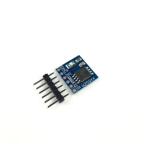
- Winbond W25Q Evaluation Board
These boards come with NB2DSK01 or pin-compatible flash devices soldered down. They provide easy access to the SPI signals and power pins. Some include an onboard microcontroller or USB interface for programming and testing the flash.
Using these evaluation platforms, developers can quickly prototype and characterize their NB2DSK01-based designs. Schematics and layout files serve as templates for custom PCBs.
SPI Flash Programming Tools
To program the NB2DSK01 flash with custom code and data, several options are available:
- Dediprog SF600 – A standalone USB programmer for various flash types
- SEGGER J-Flash – A programming tool that supports many MCUs and external flashes
- OpenOCD – Open-source programming and debugging tools with flash support
- MCU vendor IDEs – Most MCU development environments include flash programmers
When using these tools, it’s important to select the correct flash device from the configuration menus. The NB2DSK01 is compatible with the standard “M25Pxx” flash command set.
In addition to pre-built programming utilities, developers can create custom programming sequences using the NB2DSK01 instruction set. Most MCUs have built-in SPI interfaces that enable bit-banged or DMA-based flash programming.
FAQ
What is the difference between NB2DSK01 and other serial NOR flash?
The NB2DSK01 is one of many compatible serial NOR flash devices on the market. It implements a standard command set and pin-out, making it a drop-in replacement for many other 1 Mb and 2 Mb flash parts. Some key differences between vendors include:
- Maximum SPI clock frequencies
- Standby and active current specifications
- Package options and die revisions
- Extra features like unique IDs and security functions
In general, NOR flash devices are interchangeable within the same density class. The NB2DSK01 offers competitive features and performance for its class.
Can the NB2DSK01 be used for storing non-code data?
Yes, in addition to storing code, the NB2DSK01 is suitable for storing arbitrary data like configuration settings, lookup tables, fonts, images, and datalogging records. The random access nature of NOR flash allows for efficient reads and writes to any location.
What are the endurance limitations of the NB2DSK01?
The NB2DSK01 is rated for a minimum of 100,000 program/erase cycles per 4 KB sector. After this number of cumulative erasures, the flash may start to wear out and exhibit bit errors. However, by using wear leveling techniques and ECC, the lifetime can be extended substantially. For applications that perform infrequent writes, the endurance limit is unlikely to be reached during the product lifetime.
How does the NB2DSK01 compare to NAND flash?
NOR flash like the NB2DSK01 has several differences compared to NAND flash:
- NOR is byte-addressable and supports execute-in-place (XIP), while NAND is block-oriented and must be copied to RAM for execution
- NOR has lower erase/program latencies and higher random read speeds
- NAND offers higher density and lower cost-per-bit
- NOR is more reliable and has better data retention
In general, NOR is preferred for storing code and performance-critical data, while NAND is used for bulk data storage.

No responses yet