Introduction to Multilayer PCBs
Multilayer PCBs (Printed Circuit Boards) are essential components in modern electronics, enabling the complex circuitry required for advanced devices and systems. These boards consist of multiple layers of conductive and insulating materials, allowing for higher component density, improved signal integrity, and reduced electromagnetic interference (EMI). In this article, we will delve into the definition, manufacturing process, and applications of multilayer PCBs.
What is a Multilayer PCB?
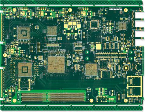
A multilayer PCB is a printed circuit board that consists of three or more conductive copper layers separated by insulating layers, typically made of FR-4 (Flame Retardant 4) material. The conductive layers are interconnected through plated through-holes (PTHs) or vias, allowing for electrical connections between different layers. This multi-layered structure enables more complex circuit designs and higher component density compared to single or double-layer PCBs.
Advantages of Multilayer PCBs
- Increased circuit density: Multilayer PCBs allow for more components and traces to be placed on a smaller board area, reducing the overall size of the device.
- Improved signal integrity: By separating signal layers with ground and power planes, multilayer PCBs minimize crosstalk and signal interference.
- Enhanced EMI shielding: The use of dedicated ground planes helps to reduce electromagnetic interference, both within the board and with external devices.
- Better heat dissipation: The increased number of copper layers improves thermal conductivity, allowing for better heat dissipation from components.
- Higher reliability: Multilayer PCBs offer improved mechanical strength and durability compared to single or double-layer boards.

Multilayer PCB Manufacturing Process
The manufacturing process for multilayer PCBs is more complex than that of single or double-layer boards, requiring precise alignment and lamination of multiple layers. The main steps involved in the manufacturing process are as follows:
-
Design and layout: The circuit design is created using PCB design software, such as Altium Designer or KiCad. The layout is optimized for signal integrity, EMI reduction, and manufacturability.
-
Material preparation: The required number of copper-clad laminates and prepreg (pre-impregnated) sheets are cut to size. Prepreg sheets are used as insulating layers between the conductive layers.
-
Drilling: Holes are drilled through the laminates and prepreg sheets to accommodate vias and component leads. High-speed CNC drilling machines ensure precise hole placement and size.
-
Layer alignment and lamination: The laminates and prepreg sheets are aligned and stacked in the proper sequence. The stack is then laminated under high pressure and temperature to fuse the layers together.
-
Plating and etching: The drilled holes are plated with copper to create electrical connections between layers. The outer layers are then patterned and etched to create the desired circuit traces.
-
Solder mask application: A solder mask is applied to the outer layers to protect the copper traces and prevent short circuits during soldering.
-
Surface finish: A surface finish, such as HASL (Hot Air Solder Leveling), ENIG (Electroless Nickel Immersion Gold), or OSP (Organic Solderability Preservative), is applied to the exposed copper areas to improve solderability and protect against oxidation.
-
Silkscreen and testing: The board’s component designators, logos, and other markings are applied using silkscreen printing. Finally, the board undergoes electrical testing to ensure proper functionality and adherence to design specifications.
Multilayer PCB Stack-Up
The stack-up of a multilayer PCB refers to the arrangement of conductive and insulating layers within the board. A typical 4-layer PCB stack-up might consist of the following layers:
| Layer | Material |
|---|---|
| Top Layer | Copper |
| Prepreg | FR-4 |
| Inner Layer 1 | Copper |
| Core | FR-4 |
| Inner Layer 2 | Copper |
| Prepreg | FR-4 |
| Bottom Layer | Copper |
The number of layers in a multilayer PCB can vary depending on the complexity of the circuit and the application requirements. Common layer counts include 4, 6, 8, 10, 12, and even higher for very complex designs.

Applications of Multilayer PCBs
Multilayer PCBs find applications in a wide range of industries and products, particularly where high component density, signal integrity, and reliability are crucial. Some key applications include:
-
Consumer electronics: Smartphones, tablets, laptops, and wearables often utilize multilayer PCBs to achieve compact, high-performance designs.
-
Telecommunications: Network switches, routers, and base stations rely on multilayer PCBs to handle high-speed data transmission and complex signal routing.
-
Automotive: Modern vehicles incorporate numerous electronic systems, such as infotainment, driver assistance, and engine control modules, which require multilayer PCBs for reliable operation in harsh environments.
-
Medical devices: Diagnostic equipment, monitoring systems, and implantable devices use multilayer PCBs to ensure high reliability and performance in critical applications.
-
Aerospace and defense: Avionics, radar systems, and satellite communications equipment employ multilayer PCBs to meet strict performance and reliability requirements in demanding environments.
-
Industrial automation: Programmable logic controllers (PLCs), human-machine interfaces (HMIs), and motor drives use multilayer PCBs for robust, high-density circuit designs.

Frequently Asked Questions (FAQ)
-
Q: What is the difference between a multilayer PCB and a single or double-layer PCB?
A: Multilayer PCBs have three or more conductive layers, while Single-Layer PCBs have one conductive layer and double-layer PCBs have two. Multilayer PCBs offer higher component density, better signal integrity, and improved EMI performance compared to single or double-layer boards. -
Q: What materials are used in the construction of multilayer PCBs?
A: Multilayer PCBs typically use copper-clad laminates for the conductive layers and FR-4 (Flame Retardant 4) material for the insulating layers. Prepreg sheets, made of partially cured FR-4, are used between the conductive layers for adhesion and insulation. -
Q: How are the layers interconnected in a multilayer PCB?
A: The layers in a multilayer PCB are interconnected through plated through-holes (PTHs) or vias. These are holes drilled through the board and plated with copper, allowing for electrical connections between different layers. -
Q: What are the advantages of using multilayer PCBs in electronic devices?
A: Multilayer PCBs offer several advantages, including increased circuit density, improved signal integrity, enhanced EMI shielding, better heat dissipation, and higher reliability compared to single or double-layer boards. -
Q: What industries commonly use multilayer PCBs in their products?
A: Multilayer PCBs are used in a wide range of industries, including consumer electronics, telecommunications, automotive, medical devices, aerospace and defense, and industrial automation. They are particularly important in applications that require high component density, signal integrity, and reliability.
Conclusion
Multilayer PCBs are a critical component in modern electronics, enabling the creation of compact, high-performance devices across various industries. By combining multiple conductive layers separated by insulating materials, multilayer PCBs offer increased circuit density, improved signal integrity, and enhanced EMI shielding compared to single or double-layer boards. The manufacturing process for multilayer PCBs involves precise alignment, lamination, drilling, plating, and etching to ensure reliable interconnections between layers. As electronic devices continue to advance in complexity and functionality, the importance of multilayer PCBs in enabling these innovations will only continue to grow.
No responses yet