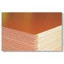
Composition and Structure of Copper Clad Laminate
Copper Foil Layer
The copper foil layer in CCL is typically made of high-purity, electrodeposited copper. The thickness of the copper foil can vary depending on the application and the desired electrical properties of the PCB. Common copper foil thicknesses include:
| Thickness (μm) | Thickness (oz) | Application |
|---|---|---|
| 18 | 0.5 | High-frequency, low-power circuits |
| 35 | 1 | General-purpose PCBs |
| 70 | 2 | High-current, power electronics |
| 105 | 3 | Extreme high-current applications |
The copper foil surface can be treated with various finishes to improve adhesion, solderability, and oxidation resistance. Some common surface treatments include:
- Electroless nickel immersion gold (ENIG)
- Immersion tin (ISn)
- Organic solderability preservative (OSP)
- Hot air solder leveling (HASL)
Dielectric Substrate
The dielectric substrate in CCL provides mechanical support and electrical insulation between the copper layers. The choice of substrate material depends on the desired electrical, thermal, and mechanical properties of the PCB. Some common substrate materials include:
- FR-4: A composite material made of woven fiberglass cloth impregnated with epoxy resin. FR-4 is the most widely used substrate material for general-purpose PCBs.
- High-Tg FR-4: A variant of FR-4 with improved thermal stability, suitable for lead-free soldering processes and high-temperature applications.
- Polyimide: A high-performance polymer with excellent thermal stability, chemical resistance, and flexibility. Polyimide is often used in flexible PCBs and high-reliability applications.
- PTFE: Polytetrafluoroethylene, also known as Teflon, is a low-loss dielectric material used in high-frequency and microwave applications.
- Ceramic: Alumina and aluminum nitride are ceramic substrates used in high-power, high-frequency, and high-temperature applications.
Manufacturing Process of Copper Clad Laminate
The manufacturing process of CCL involves several key steps:
-
Substrate Preparation: The dielectric substrate is cut to size and cleaned to remove any contaminants.
-
Copper Foil Preparation: The copper foil is also cut to size and cleaned. Surface treatments may be applied to improve adhesion and performance.
-
Lamination: The copper foil is placed on the substrate, and the stack is subjected to high pressure and temperature in a lamination press. The heat and pressure activate the adhesive, bonding the copper foil to the substrate.
-
Cooling: After lamination, the CCL is cooled to room temperature.
-
Inspection: The CCL is inspected for any defects, such as delamination, blistering, or copper foil imperfections.
-
Cutting: The CCL sheet is cut into smaller panels or boards according to customer specifications.
-
Packaging: The finished CCL products are packaged and shipped to PCB manufacturers.
Properties and Characteristics of Copper Clad Laminate
CCL exhibits several key properties and characteristics that make it suitable for PCB manufacturing:
Electrical Properties
-
Dielectric Constant (Dk): The dielectric constant is a measure of a material’s ability to store electrical energy. A lower Dk value indicates better Signal integrity and reduced signal distortion.
-
Dissipation Factor (Df): The dissipation factor represents the loss of electrical energy in the dielectric material. A lower Df value indicates better signal quality and reduced power loss.
-
Insulation Resistance: Insulation resistance is the ability of the dielectric material to resist electrical current flow between copper layers. High insulation resistance is essential to prevent short circuits and signal leakage.
Thermal Properties
-
Glass Transition Temperature (Tg): The glass transition temperature is the point at which the dielectric material transitions from a rigid, glassy state to a soft, rubbery state. A higher Tg value indicates better thermal stability and resistance to deformation during soldering processes.
-
Thermal Conductivity: Thermal conductivity is the material’s ability to conduct heat. Higher thermal conductivity helps dissipate heat generated by electronic components, improving the overall thermal management of the PCB.
-
Coefficient of Thermal Expansion (CTE): CTE is a measure of how much a material expands or contracts with changes in temperature. A lower CTE value indicates better dimensional stability and reduced stress on the copper foil and components during temperature fluctuations.
Mechanical Properties
-
Peel Strength: Peel strength is the force required to separate the copper foil from the dielectric substrate. High peel strength ensures the integrity of the copper traces and prevents delamination during PCB manufacturing and assembly.
-
Flexural Strength: Flexural strength is the ability of the CCL to resist bending and maintain its shape under mechanical stress. Higher flexural strength is essential for applications that require robust and reliable PCBs.
-
Dimensional Stability: Dimensional stability refers to the ability of the CCL to maintain its size and shape under various environmental conditions, such as temperature and humidity changes. Good dimensional stability is crucial for maintaining the accuracy of the copper trace dimensions and alignment of components.

Applications of Copper Clad Laminate
CCL is used in a wide range of electronic applications, including:
- Consumer Electronics: Smartphones, tablets, laptops, televisions, and home appliances.
- Automotive Electronics: Engine control units, infotainment systems, sensors, and power electronics for electric and hybrid vehicles.
- Industrial Electronics: Process control systems, automation equipment, power supplies, and motor drives.
- Medical Electronics: Diagnostic equipment, patient monitoring systems, and implantable devices.
- Aerospace and Defense: Avionics, radar systems, satellite communication equipment, and military-grade electronics.
- Telecommunications: Routers, switches, base stations, and wireless communication devices.
Advancements and Future Trends in Copper Clad Laminate Technology
As electronic devices continue to evolve and become more sophisticated, CCL technology must keep pace to meet the demanding requirements of the industry. Some of the advancements and future trends in CCL technology include:
High-Frequency and Low-Loss Materials
With the increasing demand for high-speed communication and data transfer, there is a growing need for CCL materials that can support high frequencies with minimal signal loss. Researchers are developing new dielectric materials and copper foil treatments that offer lower dielectric constants and dissipation factors, enabling faster signal propagation and reduced signal distortion.
Embedded Capacitance and Resistance
Embedded capacitance and resistance technologies involve incorporating passive components, such as capacitors and resistors, directly into the CCL substrate. This approach reduces the need for discrete components, saving space on the PCB and improving signal integrity. Embedded passives also simplify the PCB Assembly process and enhance the overall reliability of the electronic device.
Thermal Management Solutions
As electronic devices become more powerful and compact, thermal management becomes a critical challenge. CCL manufacturers are developing substrates with higher thermal conductivity and lower thermal expansion to help dissipate heat more effectively. Some advanced CCL products feature built-in thermal management layers, such as metal cores or heat spreaders, to further enhance thermal performance.
Environmentally Friendly Materials
There is a growing emphasis on environmentally friendly and sustainable materials in the electronics industry. CCL manufacturers are exploring the use of bio-based and recycled materials for substrates, as well as developing halogen-free flame retardants to reduce the environmental impact of PCBs. These eco-friendly initiatives not only contribute to a greener future but also help electronics manufacturers comply with increasingly stringent environmental regulations.
Frequently Asked Questions (FAQ)
-
What is the difference between single-sided and double-sided copper clad laminate?
Single-sided CCL has a copper foil layer on one side of the dielectric substrate, while double-sided CCL has copper foil on both sides. Double-sided CCL allows for more complex circuit designs and higher component density, as it enables the creation of conductive paths on both sides of the PCB. -
Can copper clad laminate be used for flexible PCBs?
Yes, CCL can be used for flexible PCBs when the dielectric substrate is a flexible material, such as polyimide. Flexible CCL allows for the creation of bendable and conformable electronic circuits that can be used in applications such as wearable devices, medical implants, and aerospace electronics. -
How does the thickness of the copper foil affect the performance of the PCB?
The thickness of the copper foil determines the current-carrying capacity and the resistance of the copper traces on the PCB. Thicker copper foil allows for higher current handling and lower resistance, which is essential for power electronics and high-current applications. However, thicker copper foil also makes it more challenging to etch fine features and increases the overall weight of the PCB. -
What is the purpose of surface treatments on copper foil?
Surface treatments on copper foil serve several purposes, including improving adhesion between the copper and the dielectric substrate, enhancing solderability for component assembly, and protecting the copper from oxidation and contamination. Common surface treatments include ENIG, OSP, and HASL, each with its own advantages and limitations. -
How does the choice of dielectric substrate material impact the performance of the CCL?
The choice of dielectric substrate material significantly influences the electrical, thermal, and mechanical properties of the CCL. For example, FR-4 is a popular choice for general-purpose PCBs due to its good balance of properties and cost-effectiveness. However, for high-frequency or high-temperature applications, materials like PTFE or ceramic may be more suitable due to their lower dielectric loss and higher thermal stability.
Conclusion
Copper Clad Laminate is a fundamental material in the production of printed circuit boards, serving as the foundation for electronic circuits in a wide range of applications. Its unique combination of a conductive copper layer and a dielectric substrate enables the creation of compact, high-performance electronic devices that have revolutionized our modern world.
As electronic technologies continue to advance, CCL manufacturers are developing innovative solutions to meet the ever-increasing demands for faster, more reliable, and more environmentally friendly electronic products. By understanding the composition, properties, and manufacturing process of CCL, engineers and designers can make informed decisions when selecting the most suitable materials for their specific applications.
With ongoing research and development in areas such as high-frequency materials, embedded passives, thermal management, and eco-friendly substrates, the future of Copper Clad Laminate looks bright. As a key enabler of electronic innovation, CCL will undoubtedly play a crucial role in shaping the electronics industry for years to come.
No responses yet