Introduction to Copper-Based Printed Circuit Boards
A printed circuit board, or PCB, is the foundational building block of most modern electronic devices. PCBs provide the physical structure to securely hold electronic components as well as the conductive pathways to electrically connect those components together into functional circuits. One of the most commonly used materials in PCB manufacturing is copper.
Copper-based PCBs leverage thin layers of copper foil laminated onto insulating substrates to create the necessary conductive traces, pads, and planes. The unique properties of copper—including its high electrical conductivity, ductility, and resistance to corrosion—make it an ideal choice for reliably carrying electrical signals between components on a PCB.
In this comprehensive article, we’ll take a deep dive into copper-based PCBs. We’ll explore:
- The composition and structure of Copper PCBs
- How copper-based PCBs are manufactured
- The benefits and applications of using copper in PCBs
- Different types of copper foils and copper weights used
- Considerations for designing with copper-based PCBs
- Frequently asked questions about copper PCBs
By the end, you’ll have a thorough understanding of the role copper plays in PCB fabrication and design. Let’s get started by examining the anatomy of a typical copper-based printed circuit board.
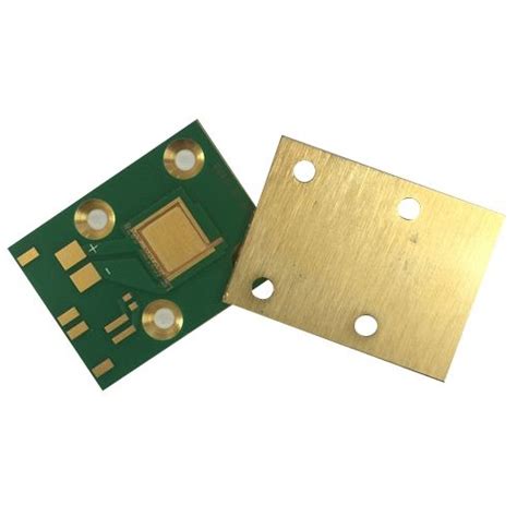
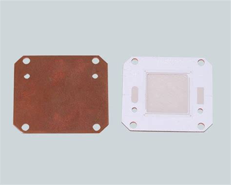
Anatomy of a Copper-Based PCB
Copper Foil Layers
The defining feature of a copper-based PCB is the use of thin copper foil sheets as the conductive material. These copper layers are laminated onto both sides of an insulating substrate, like FR-4 glass-reinforced epoxy.
A PCB can have anywhere from 1 to over 16 copper layers depending on the complexity of the design:
| Layers | PCB Type |
|---|---|
| 1 | Single-sided PCB |
| 2 | Double-sided PCB |
| 4+ | Multi-layer PCB |
The standard thickness of the copper foil used in PCBs ranges from 1 oz (35 μm) to 4 oz (140 μm). The weight is a measure of how much copper is deposited per square foot of the substrate material.
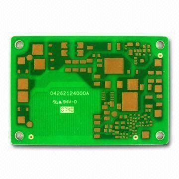
Copper Traces, Pads & Planes
During PCB manufacturing, the uniform copper foil layers are selectively etched away to form:
- Traces – thin lines that route signals between components
- Pads – surface-mount or through-hole pads for soldering components
- Planes – large copper areas used for power/ground or shielding
The width and thickness of the copper traces is an important design consideration, as it impacts the maximum current carrying capacity and characteristic impedance of the trace.
Vias & Plated Through-Holes
To facilitate electrical connections between copper layers, a copper-based PCB uses two types of vertical interconnects:
- Vias – small drilled holes that are electroplated with copper
- Plated Through-Holes (PTHs) – larger holes for mounting through-hole components
Vias come in several varieties, including standard vias that span all layers, blind vias that connect only some layers, and buried vias that are embedded within the PCB Stackup.
Solder Mask & Silkscreen
The outer copper layers of the PCB are covered with a solder mask, which is a thin polymer coating that protects the copper from oxidation and prevents solder bridges from forming during assembly.
Silkscreen is applied on top of the solder mask to add labels, logos, and other visual markings to aid in PCB Assembly and troubleshooting.
Now that we understand the basic structure, let’s look at how copper-based PCBs are actually manufactured.
How Copper-Based PCBs Are Manufactured
The PCB manufacturing process can be broken down into three main stages:
- Inner layer fabrication
- Layer stackup and lamination
- Outer layer and finish processing
Inner Layer Fabrication
For multi-layer PCBs, the inner copper layers are fabricated first:
- The base substrate material (e.g. FR-4) is cut to size
- Copper foil is laminated onto both sides using heat and pressure
- A photoresist coating is applied and then exposed to UV light through a photomask to transfer the layer’s circuit pattern
- The photoresist is developed, covering the areas that will remain as copper
- Chemical etching strips away the unmasked copper, leaving only the desired traces and pads
- The remaining photoresist is removed and the copper surface is roughened to promote adhesion
This process is repeated for each additional inner copper layer in the stackup.
PCB Stackup & Lamination
With the inner layers fabricated, they are stacked together with insulating prepreg material between each layer:
- The stackup is carefully aligned using tooling holes and registration marks
- The stackup is placed in a laminating press
- Heat and pressure bonds the layers together into a solid board
- The board is drilled to create PTHs and vias
- A chemical deposition process plates the holes with copper to form electrical connections between layers
At this stage, the outer layers are still raw copper without any circuitry.
Outer Layer Processing & Finishing
To create the circuit pattern on the outer copper layers:
- The same photoresist, exposure, etching, and stripping process used for inner layers is applied to the outer layers
- A solder mask is applied and exposed to define the opening areas for pads and vias
- Silkscreen legends are printed onto the solder mask
- A surface finish, like HASL or ENIG, is applied to protect the exposed copper pads and improve solderability
After electrical testing and final inspection, the individual PCBs are routed out of the larger manufacturing panel and packaged for shipment.
While this is a simplified overview of the fabrication process, it illustrates the central role copper plays from the initial foil lamination through to the final finish stage.

Benefits of Using Copper in PCBs
So why is copper the primary conductor of choice for PCBs? There are several key properties that make copper exceptionally well-suited for carrying electrical current in a circuit board:
High Electrical Conductivity
Copper has the second highest electrical conductivity of any element, surpassed only by silver. This allows copper traces to carry signals with minimal resistive losses.
Excellent Thermal Conductivity
In addition to conducting electricity, copper is also an excellent thermal conductor. This helps dissipate heat away from components during operation.
Corrosion Resistance
Copper naturally forms a thin protective oxide layer when exposed to air, making it resistant to further corrosion. This is important for maintaining signal integrity over the lifetime of the PCB.
Ductility & Flexibility
Copper is a relatively soft and ductile metal, meaning it can bend without breaking. This allows for some mechanical flexibility in the PCB during installation and use.
Ease of Fabrication
Copper etches uniformly and predictably, making it compatible with standard PCB manufacturing processes. It can also be easily electroplated, allowing for the creation of vias, PTHs, and even embedded copper structures.
Cost Effectiveness
While not the cheapest metal, copper provides an excellent balance of performance and cost for volume PCB manufacturing. Copper foils are a standard product with a mature supply chain.
These beneficial properties, combined with its widespread availability, have firmly established copper as the primary conducting material used in rigid PCBs.
Applications of Copper-Based PCBs
Copper-based PCBs are used across virtually every industry and electronics application, from consumer gadgets to aerospace systems. Some common applications include:
- Consumer electronics – smartphones, laptops, TVs, appliances
- Automotive – engine control units, infotainment systems, sensors
- Industrial control – PLCs, motor drives, automation equipment
- Medical devices – monitoring equipment, diagnostic tools, implantable devices
- Aerospace & defense – avionics, communications, radar systems
- IoT & wearables – smart home devices, fitness trackers, beacons
- Power electronics – inverters, power supplies, lighting controls
The specific copper weight, layer count, and layout will vary based on the electrical and mechanical requirements of each application. However, the core copper-based PCB structure remains largely consistent across these diverse use cases.
Types of Copper Used in PCBs
While the general properties of copper make it suitable for PCBs, there are actually several different types and grades of copper foil used in PCB manufacturing.
Electrodeposited (ED) Copper Foil
ED copper foil is created by electroplating copper onto a rotating stainless steel drum that is immersed in a copper sulfate solution. The copper ions are deposited onto the drum to form a thin, continuous foil.
ED copper is known for its high purity, excellent surface uniformity, and ability to produce ultra-thin foils down to ½ oz or less. It is the most commonly used type of copper foil for inner layers and flexible PCBs.
Rolled Annealed (RA) Copper Foil
RA copper foil is made by mechanically rolling copper ingots into thin sheets, which are then annealed to improve their flexibility and ductility.
Compared to ED foil, RA copper is generally less pure and has a slightly rougher surface. However, it offers higher mechanical strength and stiffness, making it a good choice for outer layers and applications with higher durability requirements.
Reverse Treated Copper Foil
Reverse treated copper foil undergoes an additional chemical etching process on the drum side to roughen the surface and improve its adhesion to the base substrate material.
This enhanced bonding strength is particularly important for high-reliability applications that may be exposed to harsh environments or thermal cycling.
Copper Weights & Thicknesses
Copper foils for PCBs are specified in terms of their weight per square foot, typically measured in ounces (oz). The most common copper weights used are:
| Copper Weight (oz/ft²) | Nominal Thickness (μm) |
|---|---|
| 0.5 | 17.5 |
| 1 | 35 |
| 2 | 70 |
| 3 | 105 |
| 4 | 140 |
The choice of copper weight depends on the specific electrical and mechanical requirements of the design. Heavier copper weights offer lower trace resistance and higher current carrying capacity, but at the cost of greater thickness and weight.
In high-frequency applications, the skin effect causes current to flow primarily on the surface of the conductor, so using a thinner copper foil can actually be advantageous for reducing signal loss.
Designing with Copper-Based PCBs
When designing a PCB layout using copper, there are several key factors to consider:
Trace Width & Thickness
The width and thickness of a copper trace will determine its resistance, current capacity, and characteristic impedance. Wider and thicker traces have lower resistance and can carry more current.
The trace width required for a given current can be calculated based on the copper weight, temperature rise, and safety margin using charts or online calculators.
Clearance & Creepage
Copper traces must be spaced far enough apart to prevent unintentional shorts or arcing. The minimum clearance between traces depends on the voltage difference and the PCB’s operating environment.
Creepage is the shortest distance between two conductors along the surface of the insulating material. It is generally larger than clearance to account for the possibility of surface contamination or degradation.
Copper Pour & Planes
Unutilized areas of the outer copper layers are typically filled with a copper pour connected to ground. This helps improve EMI shielding, reduces impedance, and provides a low-resistance return path for currents.
Inner copper layers are often dedicated entirely to power and ground planes. These large, uninterrupted copper areas distribute power evenly across the board and provide a reference plane for controlled impedance traces.
Manufacturability Constraints
PCB designers must also consider the limitations of the copper etching process when creating their layouts. Traces that are too narrow or too close together may not be consistently reproducible.
Vias and PTHs must be sized appropriately for reliable plating and drilling. Acute angles and unnecessary junctions should be avoided to prevent acid traps during etching.
By carefully considering these copper-specific design requirements, PCB designers can create layouts that are both electrically sound and readily manufacturable.
FAQ
What is the difference between copper-based and aluminum-based PCBs?
Copper is by far the most common conductive material used in rigid PCBs. However, some specialized applications may use aluminum PCBs for its lower cost and weight. The main tradeoffs with aluminum are its lower conductivity, poorer solderability, and incompatibility with standard PCB processes like Reflow Soldering. Copper remains the preferred choice for most PCB designs.
Are there any disadvantages to using copper in PCBs?
One potential drawback of copper is its relatively high cost compared to other base metals. The price of copper can fluctuate significantly based on global commodity markets. However, the superior electrical and thermal performance of copper generally outweighs any cost concerns for most PCB applications.
What is the typical lifespan of a copper-based PCB?
The lifespan of a copper-based PCB depends on many factors, including the operating environment, copper weight, surface finish, and assembly quality. In general, a well-designed and manufactured PCB can easily last for 10-20 years or more in normal use conditions. However, exposure to extreme temperatures, humidity, or chemical contamination can degrade the copper and shorten the PCB’s lifespan.
Can copper-based PCBs be recycled?
Yes, copper is a highly recyclable material. PCB recycling typically involves shredding the board and using various physical and chemical processes to separate the metals (including copper) from the other materials. The reclaimed copper can then be purified and reused in new products. Many PCB manufacturers and electronics companies have recycling programs in place to responsibly dispose of end-of-life PCBs.
Are there any emerging alternatives to copper for PCBs?
While copper is likely to remain the dominant conductor for PCBs in the near future, there is ongoing research into alternative materials that could offer improved performance or cost. One promising candidate is graphene, a two-dimensional form of carbon that has excellent electrical and thermal conductivity. However, significant challenges remain in developing scalable and cost-effective manufacturing processes for graphene-based PCBs.
Conclusion
Copper-based PCBs are the workhorse of the electronics industry, providing a reliable and efficient means of interconnecting components in a vast array of products and systems. By leveraging the unique properties of copper—its high conductivity, ductility, and resistance to corrosion—PCB designers can create boards that are both high-performing and long-lasting.
As we’ve seen, the copper foils used in PCBs come in different types, weights, and thicknesses to meet the specific requirements of each application. The PCB manufacturing process, from initial lamination through final etching and finishing, is carefully controlled to ensure the consistent quality and reliability of the copper traces and features.
When designing with copper-based PCBs, engineers must consider factors such as trace width, clearance, copper pour, and manufacturability constraints to optimize the electrical and mechanical performance of the board. By following best practices and industry standards, designers can create PCBs that are not only functional, but also efficient, reliable, and cost-effective.
While there may be some emerging alternatives on the horizon, copper is likely to remain the material of choice for PCBs for the foreseeable future. Its unique combination of properties, widespread availability, and compatibility with established manufacturing processes make it an ideal fit for the ever-evolving demands of the electronics industry.
So the next time you use your smartphone, drive your car, or fly on an airplane, remember that behind the scenes, there are countless copper-based PCBs working tirelessly to make it all possible.
No responses yet