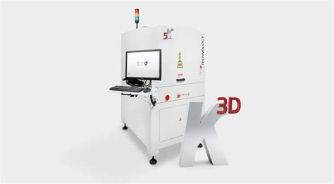
What is Automated Optical Inspection (AOI)?
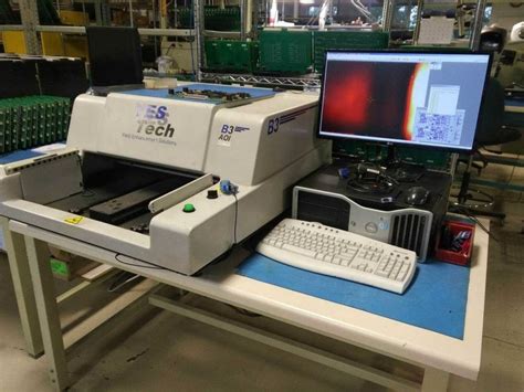
Automated Optical Inspection (AOI) is a non-contact, visual inspection method that uses cameras and image processing software to automatically detect defects in PCBs. AOI systems capture high-resolution images of the PCB and compare them to a reference image or design data to identify any discrepancies or defects. This process is highly accurate, fast, and can be performed at various stages of the PCB manufacturing process.
How does AOI work?
A typical AOI system consists of the following components:
- High-resolution cameras: One or more cameras capture detailed images of the PCB from various angles.
- Lighting system: Proper lighting is essential for capturing clear and accurate images of the PCB.
- Image processing software: Advanced algorithms analyze the captured images and compare them to the reference data to identify defects.
- Conveyor system: PCBs are transported through the AOI system for inspection.
The AOI inspection process follows these steps:
- PCB loading: The PCB is placed on the conveyor system and enters the AOI machine.
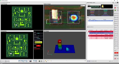
- Image capture: High-resolution cameras capture images of the PCB from various angles.
- Image processing: The captured images are analyzed by the image processing software, which compares them to the reference data.
- Defect detection: If any discrepancies or defects are found, they are flagged and reported.
- PCB unloading: The inspected PCB is unloaded from the AOI machine for further processing or repair.
Benefits of Automated Optical Inspection (AOI)
Implementing AOI in the PCB manufacturing process offers several significant benefits:
- Early defect detection: AOI can identify defects early in the manufacturing process, reducing the risk of assembling faulty PCBs into electronic devices.
- Increased productivity: AOI systems can inspect PCBs much faster than manual inspection, allowing for higher production throughput.
- Improved quality: AOI’s high accuracy and consistency ensure that PCBs meet the required quality standards, reducing the likelihood of defective products reaching customers.
- Cost savings: By detecting defects early and reducing the need for manual inspection, AOI helps minimize scrap, rework, and warranty costs.
- Traceability: AOI systems generate detailed inspection reports that can be used for traceability and process improvement purposes.
Types of Defects Detected by AOI
AOI systems can detect a wide range of PCB defects, including:
- Solder defects:
- Solder bridges
- Insufficient or excessive solder
- Cold Solder Joints
-
Component defects:
- Missing or misaligned components
- Incorrect component polarity or orientation
-
Damaged or lifted components
-
Trace and pad defects:
- Open or short circuits
- Trace width or spacing violations
-
Damaged or lifted pads
-
Artwork and legend defects:
- Incorrect or missing text or graphics
-
Alignment or registration issues
-
Contamination and foreign material:
- Flux residue
- Dust or debris
- Scratches or stains

AOI in the PCB Manufacturing Process
AOI is typically performed at multiple stages of the PCB manufacturing process to ensure the highest quality standards are met.
Bare Board AOI
Bare board AOI is performed after the PCB fabrication process and before component assembly. It inspects the bare PCB for defects such as:
- Trace and pad integrity
- Drill hole size and position
- Solder mask and silkscreen alignment
- Copper thickness and uniformity
Pre-Reflow AOI
Pre-reflow AOI is performed after component placement but before the soldering process. It checks for defects such as:
- Component presence and alignment
- Solder paste coverage and volume
- Solder paste registration and offset
Post-Reflow AOI
Post-reflow AOI is performed after the soldering process and before final assembly. It inspects for defects such as:
- Solder joint quality
- Component presence and alignment
- Solder bridging or shorts
- Insufficient or excessive solder
Comparison of AOI Inspection Stages
| Inspection Stage | Defects Detected | Benefits |
|---|---|---|
| Bare Board AOI | – Trace and pad integrity – Drill hole size and position – Solder mask and silkscreen alignment – Copper thickness and uniformity |
– Early detection of PCB fabrication defects – Prevents defective PCBs from entering assembly process |
| Pre-Reflow AOI | – Component presence and alignment – Solder paste coverage and volume – Solder paste registration and offset |
– Identifies component placement and solder paste issues before soldering – Reduces the risk of soldering defects |
| Post-Reflow AOI | – Solder joint quality – Component presence and alignment – Solder bridging or shorts – Insufficient or excessive solder |
– Detects soldering defects before final assembly – Ensures PCB functionality and reliability |
Implementing AOI in PCB Manufacturing
To successfully implement AOI in a PCB manufacturing process, consider the following factors:
- Select the appropriate AOI system based on your specific requirements, such as PCB Complexity, production volume, and defect types.
- Develop a comprehensive library of reference images and design data for each PCB type to ensure accurate defect detection.
- Establish clear quality standards and acceptance criteria for each inspection stage.
- Train operators on the proper use and maintenance of the AOI system to ensure consistent and reliable results.
- Regularly review and analyze AOI data to identify process improvement opportunities and track quality trends.
Frequently Asked Questions (FAQ)
-
Q: Can AOI replace manual visual inspection entirely?
A: While AOI is highly accurate and efficient, it is often used in conjunction with manual visual inspection for critical or complex PCBs. Manual inspection can catch certain defects that AOI may miss, such as subtle cosmetic issues or defects not included in the AOI system’s defect library. -
Q: How does AOI differ from X-ray inspection?
A: AOI is a visual inspection method that uses cameras to detect surface-level defects, while X-ray inspection uses X-rays to detect internal defects, such as voids or cracks in solder joints. X-ray inspection is often used for high-density or multi-layer PCBs where AOI may not be sufficient. -
Q: Can AOI detect all types of PCB defects?
A: While AOI can detect a wide range of defects, it may not catch every issue. Some defects, such as internal voids or subtle cosmetic issues, may require additional inspection methods like X-ray or manual visual inspection. -
Q: How does the speed of AOI compare to manual inspection?
A: AOI systems can inspect PCBs much faster than manual inspection, often at rates of several thousand components per minute. This high-speed inspection allows for increased production throughput and faster time-to-market. -
Q: What factors should be considered when selecting an AOI system?
A: When choosing an AOI system, consider factors such as PCB complexity, production volume, defect types, speed requirements, and budget. It’s essential to select a system that can accurately detect the defects specific to your PCBs and integrate seamlessly into your manufacturing process.
Conclusion
Automated Optical Inspection (AOI) is a critical quality control process in PCB manufacturing that uses high-resolution cameras and advanced image processing software to detect defects. By implementing AOI at various stages of the manufacturing process, companies can improve product quality, increase productivity, and reduce costs. As PCBs continue to become more complex and miniaturized, the role of AOI in ensuring their reliability and functionality will only grow in importance.
No responses yet