Introduction to Microwave PCBs
Microwave PCBs, or Printed Circuit Boards, are specialized boards designed to operate at high frequencies, typically in the range of 300 MHz to 300 GHz. These PCBs are essential components in various microwave applications, such as radar systems, wireless communications, and satellite technology. The unique properties of microwave PCBs enable them to handle high-frequency signals efficiently while minimizing signal loss and interference.
Key Characteristics of Microwave PCBs
-
High-Frequency Operation: Microwave PCBs are engineered to function at extremely high frequencies, allowing for the transmission and reception of microwave signals.
-
Low Dielectric Loss: The materials used in microwave PCBs, such as PTFE (Polytetrafluoroethylene) and Rogers laminates, have low dielectric loss, which minimizes signal attenuation and ensures signal integrity.
-
Controlled Impedance: Microwave PCBs are designed with controlled impedance to match the impedance of the connected components and prevent signal reflections.
-
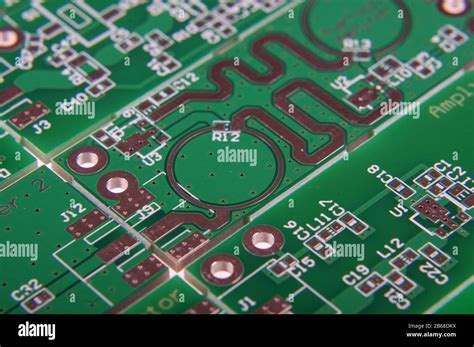
Specialized Trace Geometries: The traces on microwave PCBs are carefully designed using techniques like microstrip, stripline, and coplanar waveguide to optimize signal propagation and minimize losses.
Microwave PCB Materials
The choice of materials is crucial in the design and fabrication of microwave PCBs. The materials used must have specific properties to ensure optimal performance at high frequencies.
Common Microwave PCB Materials
| Material | Dielectric Constant | Dissipation Factor | Thermal Conductivity (W/mK) |
|---|---|---|---|
| PTFE | 2.1 | 0.0002 | 0.25 |
| Rogers RO4003C | 3.38 | 0.0027 | 0.71 |
| Rogers RO4350B | 3.48 | 0.0037 | 0.69 |
| Alumina | 9.9 | 0.0001 | 24 |
-
PTFE (Polytetrafluoroethylene): PTFE, also known as Teflon, is a popular choice for microwave PCBs due to its low dielectric loss and stable dielectric constant over a wide frequency range.
-
Rogers Laminates: Rogers Corporation offers a range of high-performance laminates, such as RO4003C and RO4350B, which are specifically designed for microwave applications. These materials provide excellent electrical properties and thermal stability.
-
Alumina: Alumina, or aluminum oxide, is a ceramic material used in high-power microwave applications due to its high thermal conductivity and low dielectric loss.

Microwave PCB Design Considerations
Designing microwave PCBs requires careful consideration of several factors to ensure optimal performance and signal integrity.
Key Design Considerations
-
Impedance Matching: Proper impedance matching is essential to minimize signal reflections and ensure maximum power transfer. The PCB traces must be designed with the correct width and spacing to achieve the desired characteristic impedance.
-
Transmission Line Structures: Microwave PCBs employ various transmission line structures, such as microstrip, stripline, and coplanar waveguide, to guide the high-frequency signals. Each structure has its own advantages and limitations, and the choice depends on the specific application and design requirements.
-
Grounding and Shielding: Proper grounding and shielding techniques are crucial in microwave PCB design to minimize electromagnetic interference (EMI) and crosstalk. This includes the use of ground planes, via stitching, and shielding enclosures.
-
Component Placement: The placement of components on a microwave PCB is critical to minimizing signal path lengths and reducing parasitic effects. Components should be placed as close as possible to their associated traces to minimize discontinuities and reflections.
-
Via Optimization: Vias in microwave PCBs can introduce discontinuities and signal loss. Therefore, via optimization techniques, such as via-in-pad and blind/buried vias, are employed to minimize their impact on signal integrity.

Microwave PCB Fabrication Process
The fabrication process for microwave PCBs is more complex and demanding compared to standard PCBs due to the high-frequency requirements and specialized materials used.
Key Steps in Microwave PCB Fabrication
-
Material Selection: The appropriate microwave PCB material is selected based on the desired electrical properties, thermal stability, and mechanical requirements.
-
Artwork Generation: The PCB layout is designed using specialized CAD software, taking into account the microwave-specific design considerations mentioned earlier.
-
Lamination: The PCB layers are laminated together under high pressure and temperature to form a cohesive board.
-
Drilling: Holes are drilled into the laminated board for vias and component mounting.
-
Plating: The drilled holes are plated with copper to establish electrical connections between layers.
-
Etching: The unwanted copper is etched away, leaving behind the desired trace patterns.
-
Solder Mask Application: A solder mask is applied to protect the traces and prevent short circuits.
-
Surface Finish: A surface finish, such as ENIG (Electroless Nickel Immersion Gold) or HASL (Hot Air Solder Leveling), is applied to the exposed copper areas to improve solderability and protect against oxidation.
-
Electrical Testing: The fabricated microwave PCB undergoes rigorous electrical testing to ensure it meets the specified performance requirements.

Applications of Microwave PCBs
Microwave PCBs find applications in various industries and sectors where high-frequency signal processing is required.
Key Application Areas
-
Telecommunications: Microwave PCBs are used in wireless communication systems, such as 5G networks, satellite communications, and point-to-point links.
-
Radar Systems: Microwave PCBs are essential components in radar systems for defense, aerospace, and automotive applications.
-
Aerospace and Defense: Microwave PCBs are used in avionics, missile guidance systems, and electronic warfare equipment.
-
Medical Devices: Microwave PCBs are employed in medical imaging systems, such as MRI machines and microwave ablation devices.
-
Scientific Instruments: High-frequency test and measurement equipment, such as network analyzers and spectrum analyzers, rely on microwave PCBs for accurate signal processing.
Challenges and Future Trends
The design and fabrication of microwave PCBs present several challenges, and the industry is continuously evolving to address these challenges and meet the growing demands of high-frequency applications.
Challenges in Microwave PCB Design and Fabrication
-
Signal Integrity: Maintaining signal integrity at high frequencies is a significant challenge due to the increased susceptibility to losses, reflections, and interference.
-
Material Limitations: The availability of suitable materials with the required electrical and thermal properties can be limited, and the cost of specialized materials can be high.
-
Manufacturing Complexity: The fabrication process for microwave PCBs is more complex and requires specialized equipment and expertise, leading to higher manufacturing costs.
Future Trends in Microwave PCB Technology
-
Advanced Materials: The development of new materials with improved electrical and thermal properties will enable the design of microwave PCBs with higher performance and reliability.
-
3D Printing: The adoption of 3D printing technologies for microwave PCB fabrication can offer greater design flexibility and faster prototyping.
-
Integration with RF Components: The integration of microwave PCBs with RF components, such as antennas and filters, will enable the development of more compact and efficient high-frequency systems.
-
Higher Frequencies: As the demand for higher data rates and bandwidth increases, microwave PCBs will need to operate at even higher frequencies, pushing the boundaries of current technologies.
Frequently Asked Questions (FAQ)
-
What is the difference between a microwave PCB and a standard PCB?
A microwave PCB is specifically designed to operate at high frequencies (300 MHz to 300 GHz), while a standard PCB is designed for lower frequency applications. Microwave PCBs use specialized materials and design techniques to minimize signal loss and ensure signal integrity at high frequencies. -
What materials are commonly used in microwave PCBs?
Common materials used in microwave PCBs include PTFE (Polytetrafluoroethylene), Rogers laminates (such as RO4003C and RO4350B), and Alumina. These materials have low dielectric loss and stable dielectric constants, which are essential for high-frequency performance. -
Why is impedance matching important in microwave PCB design?
Impedance matching is crucial in microwave PCB design to minimize signal reflections and ensure maximum power transfer. Mismatched impedances can lead to signal degradation, reduced efficiency, and potential damage to connected components. -
What are the key design considerations for microwave PCBs?
Key design considerations for microwave PCBs include impedance matching, transmission line structures (microstrip, stripline, coplanar waveguide), grounding and shielding, component placement, and via optimization. These factors are critical to maintaining signal integrity and minimizing losses at high frequencies. -
What are the main applications of microwave PCBs?
Microwave PCBs find applications in various industries, including telecommunications (5G networks, satellite communications), radar systems, aerospace and defense (avionics, missile guidance), medical devices (MRI machines, microwave ablation), and scientific instruments (network analyzers, spectrum analyzers).
Conclusion
Microwave PCBs are critical components in high-frequency applications, enabling the transmission and processing of signals in the range of 300 MHz to 300 GHz. The unique properties of microwave PCBs, such as low dielectric loss, controlled impedance, and specialized trace geometries, make them essential for maintaining signal integrity and minimizing losses in microwave systems.
The design and fabrication of microwave PCBs require careful consideration of materials, impedance matching, transmission line structures, grounding, and shielding. As the demand for high-frequency applications continues to grow, advancements in materials, manufacturing processes, and integration techniques will shape the future of microwave PCB technology.
By understanding the fundamentals of microwave PCBs, designers and engineers can develop high-performance systems that meet the stringent requirements of microwave applications in telecommunications, radar, aerospace, medical devices, and scientific instrumentation.
No responses yet