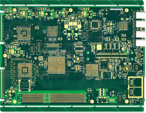
Introduction to Multilayer PCBs
Printed Circuit Boards (PCBs) are the backbone of modern electronics. They provide a platform for components to be mounted and connected, forming a complete electronic circuit. As technology advances and devices become more complex, the demand for higher density and more efficient PCBs has led to the development of multilayer PCBs. Among these, the 6 layer PCB board has gained popularity due to its ability to accommodate complex designs while maintaining a compact form factor.
What is a Multilayer PCB?
A multilayer PCB is a printed circuit board that consists of three or more conductive copper layers separated by insulating layers. These layers are laminated together using heat and pressure to form a single board. The conductive layers are interconnected through vias, which are small holes drilled through the board and plated with conductive material.
Advantages of Multilayer PCBs
Multilayer PCBs offer several advantages over single or double-layer boards:
- Increased density: Multilayer PCBs allow for more components and traces to be placed on a single board, reducing the overall size of the device.
- Improved signal integrity: By separating signals on different layers, multilayer PCBs reduce crosstalk and electromagnetic interference (EMI).
- Enhanced thermal management: The additional layers can be used to dissipate heat more efficiently, improving the overall performance and reliability of the device.
- Reduced cost: Although the initial cost of fabricating a multilayer PCB may be higher, the increased density and functionality often result in cost savings in the long run.
The 6 Layer PCB Board
What is a 6 Layer PCB?
A 6 layer PCB is a type of multilayer PCB that consists of six conductive layers separated by insulating layers. These layers are typically arranged in a specific order to optimize signal integrity and power distribution. The most common stack-up for a 6 layer PCB is as follows:
| Layer | Function |
|---|---|
| Top Layer | Signal and components |
| Ground Layer | Ground plane |
| Inner Layer 1 | Signal |
| Inner Layer 2 | Signal |
| Power Layer | Power plane |
| Bottom Layer | Signal and components |
Applications of 6 Layer PCBs
Six layer PCBs are commonly used in a wide range of applications, including:
- Telecommunications equipment
- Medical devices
- Aerospace and defense systems
- High-performance computing
- Automotive electronics
- Industrial control systems
The increased density and signal integrity provided by 6 layer PCBs make them ideal for devices that require high-speed data transmission, such as 5G networks and high-performance computing systems.
Design Considerations for 6 Layer PCBs
Designing a 6 layer PCB requires careful consideration of several factors to ensure optimal performance and reliability. Some key design considerations include:
- Signal integrity: Proper routing and layer arrangement are crucial to maintaining signal integrity. Signals should be separated on different layers to minimize crosstalk and EMI.
- Power distribution: The power layer should be designed to provide a stable and clean power supply to all components on the board. Decoupling capacitors should be placed close to power-hungry components to reduce noise and ensure a stable power supply.
- Thermal management: The layout of the board should be designed to facilitate efficient heat dissipation. This may involve the use of thermal vias, heat sinks, or other cooling methods.
- Manufacturing constraints: The design must adhere to the manufacturing capabilities of the PCB fabricator. This includes minimum trace widths, hole sizes, and spacing between components.
Fabrication Process for 6 Layer PCBs
The fabrication process for a 6 layer PCB involves several steps:
- Design and layout: The circuit is designed using CAD software, and the layout is created to specify the placement of components and routing of traces.
- Layer preparation: Each conductive layer is prepared by printing the circuit pattern onto a thin sheet of copper foil.
- Lamination: The conductive layers are separated by insulating layers and laminated together using heat and pressure to form a single board.
- Drilling: Holes are drilled through the board to accommodate vias and component leads.
- Plating: The holes are plated with conductive material to create electrical connections between layers.
- Etching: The unwanted copper is removed using a chemical etching process, leaving only the desired circuit pattern.
- Solder mask and silkscreen: A protective solder mask is applied to the board, and a silkscreen layer is added to label components and provide assembly instructions.
- Surface finish: A surface finish, such as HASL or ENIG, is applied to protect the exposed copper and facilitate soldering.
Benefits of Using 6 Layer PCBs
Using a 6 layer PCB offers several benefits over fewer layer boards:
- Increased functionality: The additional layers allow for more complex circuits and higher component density, enabling more features and functions to be incorporated into a single device.
- Improved signal integrity: By separating signals on different layers and using dedicated ground and power planes, 6 layer PCBs can significantly reduce crosstalk and EMI, resulting in cleaner and more reliable signals.
- Better thermal management: The increased number of layers provides more paths for heat dissipation, allowing for better thermal management and improved overall performance.
- Reduced size and weight: The higher density and functionality of 6 layer PCBs enable devices to be made smaller and lighter, which is particularly important in applications such as aerospace and portable electronics.
Challenges and Considerations
Despite the many benefits of 6 layer PCBs, there are also some challenges and considerations to keep in mind:
- Higher cost: The increased complexity and number of layers make 6 layer PCBs more expensive to fabricate than fewer layer boards.
- Design complexity: Designing a 6 layer PCB requires more expertise and attention to detail to ensure proper signal integrity and power distribution.
- Manufacturing challenges: The increased number of layers and smaller feature sizes can make 6 layer PCBs more difficult to manufacture, requiring more advanced equipment and processes.
- Testing and inspection: With more layers and higher density, testing and inspecting 6 layer PCBs can be more challenging and time-consuming.

Frequently Asked Questions (FAQ)
-
Q: What is the difference between a 4 layer and a 6 layer PCB?
A: A 4 layer PCB has four conductive layers, typically arranged as signal-ground-signal-signal, while a 6 layer PCB has six conductive layers, usually arranged as signal-ground-signal-signal-power-signal. The additional layers in a 6 layer PCB provide more space for routing and better signal integrity. -
Q: When should I choose a 6 layer PCB over a 4 layer PCB?
A: A 6 layer PCB is generally recommended when the circuit design is complex, requires high-speed signals, or needs better power distribution and thermal management. If your design has a high component density or requires multiple power supplies, a 6 layer PCB may be the better choice. -
Q: Are 6 layer PCBs more expensive than 4 layer PCBs?
A: Yes, 6 layer PCBs are generally more expensive to fabricate than 4 layer PCBs due to the increased complexity and number of layers. However, the improved functionality and performance of a 6 layer PCB can often justify the higher cost. -
Q: Can I use a 6 layer PCB for low-speed designs?
A: While 6 layer PCBs are often used for high-speed designs, they can also be used for low-speed applications. The additional layers can provide better power distribution and noise reduction, which can be beneficial even in low-speed circuits. -
Q: What are the typical applications for 6 layer PCBs?
A: Six layer PCBs are commonly used in a wide range of applications, including telecommunications equipment, medical devices, aerospace and defense systems, high-performance computing, automotive electronics, and industrial control systems. They are particularly well-suited for devices that require high-speed data transmission, complex functionality, and compact form factors.

Conclusion
Six layer PCBs are a powerful tool for creating complex, high-performance electronic devices. By providing increased density, improved signal integrity, better thermal management, and reduced size and weight, 6 layer PCBs enable designers to push the boundaries of what is possible in modern electronics.
However, designing and manufacturing 6 layer PCBs also comes with its own set of challenges and considerations. Designers must carefully balance the benefits of increased functionality with the higher costs and complexity associated with 6 layer boards.
As technology continues to advance and the demand for more powerful, compact, and reliable electronic devices grows, the use of 6 layer PCBs and other multilayer boards is likely to become increasingly common. By understanding the principles, benefits, and challenges of 6 layer PCBs, designers and engineers can make informed decisions about when and how to use these powerful tools to create the next generation of electronic devices.

No responses yet