How Vias Affect Signal Integrity in High-Speed PCIe Designs
PCI Express (PCIe) has become the dominant interconnect standard for high-speed communication in computers and other electronic devices. As PCIe data rates continue to increase with each new generation, maintaining signal integrity becomes more challenging, especially when signals need to traverse between different layers of a printed circuit board (PCB) using vias.
This article explores the impact of layer changing vias on signal integrity when using PCIe at higher speeds and discusses strategies for mitigating via-related issues to ensure robust and reliable PCIe communication.
Understanding Vias and Their Role in PCB Design
Vias are conductive pathways that allow signals to pass through different layers of a PCB. There are several types of vias:
- Through-hole vias: These vias go through the entire thickness of the PCB.
- Blind vias: These vias connect an outer layer to an inner layer but do not go through the entire board.
- Buried vias: These vias connect inner layers without reaching either outer layer.
In high-speed PCB designs, such as those using PCIe, vias are essential for routing signals between layers to achieve efficient use of board space and minimize signal path lengths. However, vias can also introduce discontinuities and impedance mismatches that degrade signal integrity.
The Impact of Layer Changing Vias on PCIe Signal Integrity
As PCIe data rates increase, the impact of layer changing vias on signal integrity becomes more pronounced. The primary issues caused by vias include:
-
Impedance discontinuities: Vias can create impedance discontinuities due to changes in the signal path geometry, leading to reflections and degraded signal quality.
-
Stub resonances: Unused portions of through-hole vias (via stubs) can act as resonant circuits, causing signal distortion and limiting the maximum usable frequency.
-
Crosstalk: Vias can couple noise from adjacent signal paths, resulting in crosstalk that can corrupt data and reduce signal-to-noise ratio (SNR).
-
Increased insertion loss: Vias add series inductance and shunt capacitance to the signal path, increasing insertion loss and limiting the maximum achievable data rate.
The table below summarizes the impact of layer changing vias on PCIe signal integrity at different data rates:
| PCIe Generation | Data Rate (GT/s) | Via Impact on Signal Integrity |
|---|---|---|
| Gen 1 | 2.5 | Low |
| Gen 2 | 5.0 | Moderate |
| Gen 3 | 8.0 | High |
| Gen 4 | 16.0 | Very High |
| Gen 5 | 32.0 | Extremely High |
As the table illustrates, the impact of vias on signal integrity increases significantly with each new PCIe generation, making via optimization crucial for maintaining reliable communication at higher speeds.
Strategies for Mitigating Via-Related Signal Integrity Issues
To mitigate the impact of layer changing vias on PCIe signal integrity, PCB designers can employ several strategies:
- Via optimization:
- Minimize via count and via stubs by using blind and buried vias where possible.
- Optimize via geometry (diameter, pad size, and antipad size) to minimize impedance discontinuities.
-
Use via stitching to create a continuous return path and reduce impedance mismatch.
-
Impedance matching:
- Use controlled impedance vias and traces to maintain a consistent characteristic impedance throughout the signal path.
-
Implement differential vias for differential signaling to minimize common-mode noise and improve signal integrity.
-
Ground plane optimization:
- Ensure adequate ground plane coverage and proper via spacing to minimize crosstalk and provide a low-impedance return path.
-
Use guard vias or ground vias to isolate sensitive signals and reduce coupling between adjacent vias.
-
Signal conditioning:
- Implement equalization techniques, such as pre-emphasis and de-emphasis, to compensate for via-related signal degradation.
-
Use continuous time linear equalization (CTLE) and decision feedback equalization (DFE) to improve signal quality and extend the maximum achievable data rate.
-
Simulation and validation:
- Perform signal integrity simulations to predict via performance and optimize design parameters.
- Validate via performance through measurements and testing to ensure compliance with PCIe specifications.
By applying these strategies, PCB designers can effectively mitigate the impact of layer changing vias on PCIe signal integrity and ensure reliable communication at higher data rates.
Case Study: Optimizing Vias for PCIe Gen 5
To illustrate the importance of via optimization in high-speed PCIe designs, let’s consider a case study involving the implementation of PCIe Gen 5, which operates at a data rate of 32 GT/s.
In this case study, a PCB designer is tasked with designing a motherboard that supports PCIe Gen 5 communication between the CPU and multiple peripheral devices. The design requires numerous layer changing vias to route signals between the CPU, PCIe slots, and other components.
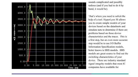
The designer begins by performing signal integrity simulations to evaluate the impact of different via configurations on PCIe Gen 5 signal quality. The simulations reveal that using standard through-hole vias results in significant impedance discontinuities and stub resonances, leading to unacceptable levels of signal distortion and degradation.
To address these issues, the designer optimizes the via geometry by reducing the via diameter and pad size while increasing the antipad size. Additionally, blind and buried vias are used to minimize via stubs and reduce the overall via count.
The designer also implements differential vias for the PCIe differential pairs to minimize common-mode noise and improve signal integrity. Ground vias are strategically placed to provide a low-impedance return path and reduce crosstalk between adjacent signal vias.
After applying these optimizations, the designer reruns the signal integrity simulations and finds that the optimized via configuration significantly improves PCIe Gen 5 signal quality, with reduced impedance discontinuities, minimized stub resonances, and improved eye diagram openings.
The optimized design is then validated through measurements and testing, confirming that the PCIe Gen 5 signals meet the required specifications for reliable communication.
This case study demonstrates the critical role of via optimization in enabling the successful implementation of high-speed PCIe communication and highlights the importance of simulation, optimization, and validation in the PCB design process.
Frequently Asked Questions (FAQ)
- What are the main types of vias used in PCB design?
- Through-hole vias: These vias go through the entire thickness of the PCB.
- Blind vias: These vias connect an outer layer to an inner layer but do not go through the entire board.
-
Buried vias: These vias connect inner layers without reaching either outer layer.
-
How do vias affect signal integrity in high-speed PCIe designs?
Vias can introduce several issues that degrade signal integrity in high-speed PCIe designs, including: - Impedance discontinuities due to changes in the signal path geometry.
- Stub resonances caused by unused portions of through-hole vias.
- Crosstalk resulting from coupling between adjacent signal vias.
-
Increased insertion loss due to added series inductance and shunt capacitance.
-
What strategies can be used to mitigate via-related signal integrity issues in PCIe designs?
Strategies for mitigating via-related signal integrity issues include: - Via optimization: Minimizing via count and stubs, optimizing via geometry, and using via stitching.
- Impedance matching: Using controlled impedance vias and traces and implementing differential vias.
- Ground plane optimization: Ensuring adequate ground plane coverage and proper via spacing.
- Signal conditioning: Implementing equalization techniques like pre-emphasis, de-emphasis, CTLE, and DFE.
-
Simulation and validation: Performing signal integrity simulations and validating via performance through measurements and testing.
-
Why is via optimization particularly important for PCIe Gen 5 and beyond?
As PCIe data rates continue to increase with each new generation, the impact of vias on signal integrity becomes more pronounced. For PCIe Gen 5, which operates at 32 GT/s, via optimization is crucial to maintain reliable communication and ensure compliance with the standard’s specifications. Failure to optimize vias can result in significant signal distortion, degradation, and ultimately, communication failures. -
How can PCB designers ensure their via optimizations are effective?
PCB designers can ensure the effectiveness of their via optimizations by: - Performing comprehensive signal integrity simulations to predict via performance and optimize design parameters.
- Validating via performance through measurements and testing to confirm compliance with PCIe specifications.
- Staying up-to-date with industry best practices and guidelines for via design in high-speed applications.
- Collaborating with signal integrity experts and leveraging their knowledge and experience in via optimization techniques.
By understanding the impact of vias on signal integrity and applying appropriate optimization strategies, PCB designers can successfully implement high-speed PCIe communication in their designs, enabling the development of faster, more reliable electronic devices.
No responses yet