Introduction to PCIe 5.0 and Its Importance in Modern Computing
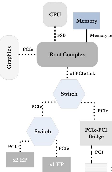
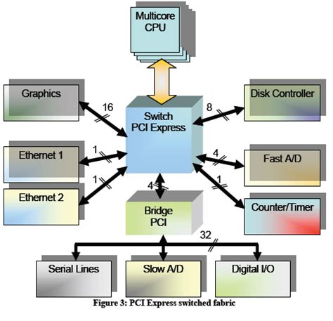
PCIe (Peripheral Component Interconnect Express) is a high-speed serial computer expansion bus standard that has been widely adopted in modern computing systems. It is used to connect various components, such as graphics cards, solid-state drives, and network adapters, to the motherboard. The latest version, PCIe 5.0, offers significant improvements in terms of bandwidth, power efficiency, and features compared to its predecessors.
PCIe 5.0 doubles the bandwidth of PCIe 4.0, providing a raw data rate of 32 GT/s (gigatransfers per second) and a maximum throughput of 128 GB/s for a x16 configuration. This increased bandwidth is crucial for demanding applications, such as high-performance gaming, artificial intelligence, and data centers.
Key Features of PCIe 5.0
- Doubled bandwidth compared to PCIe 4.0
- Improved power efficiency
- Backward compatibility with previous PCIe versions
- Enhanced reliability and error correction mechanisms
- Support for new features, such as PCIe 5.0 PIPE (Physical Interface for PCI Express)
Challenges in PCIe 5.0 Layout and Routing
Designing a PCB (Printed Circuit Board) for PCIe 5.0 presents several challenges due to the high-speed nature of the interface. Some of the key challenges include:
Signal Integrity
Signal integrity is a critical aspect of PCIe 5.0 layout and routing. The high-speed signals are susceptible to various issues, such as crosstalk, reflections, and attenuation. To ensure proper signal integrity, designers must carefully consider factors such as trace geometry, impedance matching, and via design.
Power Integrity
PCIe 5.0 devices consume significant amounts of power, which can lead to power integrity issues if not properly managed. Designers must ensure that the power delivery network (PDN) is robust enough to handle the current requirements of the PCIe 5.0 device while minimizing voltage ripple and noise.
Electromagnetic Interference (EMI)
The high-speed signals in PCIe 5.0 can generate electromagnetic interference (EMI), which can affect the performance of nearby components and cause compliance issues. Designers must implement appropriate EMI mitigation techniques, such as proper grounding, shielding, and filtering, to minimize EMI.
Thermal Management
PCIe 5.0 devices generate significant amounts of heat, which must be effectively dissipated to ensure reliable operation. Designers must consider thermal management strategies, such as heatsinks, fans, and thermal vias, to prevent overheating and ensure optimal performance.

Best Practices for PCIe 5.0 Layout and Routing
To overcome the challenges associated with PCIe 5.0 layout and routing, designers should follow best practices and guidelines. Some of the key best practices include:
Impedance Matching and Trace Geometry
Proper impedance matching is crucial for maintaining signal integrity in PCIe 5.0 designs. Traces should be designed with a characteristic impedance of 85 Ω ± 10% for single-ended signals and 100 Ω ± 10% for differential pairs. Trace geometry, including width, spacing, and length matching, should be carefully controlled to minimize reflections and crosstalk.
Via Design and Optimization
Vias are essential for connecting traces on different layers of the PCB but can also introduce discontinuities and reflections. Designers should optimize via design by using techniques such as back-drilling, via-in-pad, and microvias to minimize the impact of vias on signal integrity.
Power Delivery Network (PDN) Design
A robust power delivery network is essential for maintaining power integrity in PCIe 5.0 designs. Designers should use appropriate decoupling capacitors, power planes, and voltage regulators to ensure stable and clean power supply to the PCIe 5.0 device. Simulations and analysis tools can be used to optimize the PDN design and minimize voltage ripple and noise.
EMI Mitigation Techniques
To minimize electromagnetic interference, designers should implement appropriate EMI mitigation techniques. These include proper grounding, shielding, and filtering of high-speed signals. Spread-spectrum clocking and differential signaling can also help reduce EMI emissions.
Thermal Management Strategies
Effective thermal management is crucial for ensuring reliable operation of PCIe 5.0 devices. Designers should incorporate thermal management strategies, such as heatsinks, fans, and thermal vias, to dissipate heat generated by the device. Thermal simulations and analysis tools can be used to optimize the thermal design and ensure that the device operates within its specified temperature range.

Tools and Methodologies for PCIe 5.0 Layout and Routing
To effectively design PCBs for PCIe 5.0, designers rely on various tools and methodologies. Some of the essential tools and methodologies include:
PCB Design Software
Advanced PCB design software, such as Cadence Allegro, Mentor Graphics Xpedition, and Altium Designer, provide features specifically tailored for high-speed design and PCIe layout. These tools offer capabilities such as constraint-driven routing, signal integrity analysis, and 3D visualization to help designers create optimal PCIe 5.0 layouts.
Simulation and Analysis Tools
Simulation and analysis tools are essential for verifying the performance of PCIe 5.0 designs before fabrication. Tools such as Keysight ADS, Ansys HFSS, and Cadence Sigrity enable designers to simulate and analyze signal integrity, power integrity, and EMI performance of their designs. These tools help identify potential issues early in the design process, reducing the risk of costly redesigns.
Collaboration and Design Review
Effective collaboration and design review processes are crucial for ensuring the success of PCIe 5.0 projects. Designers should work closely with other team members, such as signal integrity engineers, power integrity engineers, and mechanical designers, to ensure that all aspects of the design are properly integrated. Regular design reviews help catch potential issues early and ensure that the design meets all requirements.

FAQs
What is the difference between PCIe 5.0 and previous versions?
PCIe 5.0 doubles the bandwidth of PCIe 4.0, providing a raw data rate of 32 GT/s and a maximum throughput of 128 GB/s for a x16 configuration. It also offers improved power efficiency, backward compatibility, and support for new features such as PCIe 5.0 PIPE.
What are the main challenges in PCIe 5.0 layout and routing?
The main challenges in PCIe 5.0 layout and routing include signal integrity, power integrity, electromagnetic interference (EMI), and thermal management. Designers must carefully consider factors such as trace geometry, impedance matching, via design, power delivery network design, EMI mitigation techniques, and thermal management strategies to ensure optimal performance and reliability.
What tools are used for PCIe 5.0 layout and routing?
Advanced PCB design software, such as Cadence Allegro, Mentor Graphics Xpedition, and Altium Designer, are used for PCIe 5.0 layout and routing. Simulation and analysis tools, such as Keysight ADS, Ansys HFSS, and Cadence Sigrity, are used to verify the performance of PCIe 5.0 designs before fabrication.
How can designers ensure signal integrity in PCIe 5.0 designs?
Designers can ensure signal integrity in PCIe 5.0 designs by properly matching impedances, optimizing trace geometry, carefully designing vias, and using appropriate termination techniques. Simulation and analysis tools can be used to identify and mitigate potential signal integrity issues.
What are some best practices for PCIe 5.0 layout and routing?
Some best practices for PCIe 5.0 layout and routing include proper impedance matching and trace geometry, via design and optimization, robust power delivery network design, EMI mitigation techniques, and effective thermal management strategies. Collaboration and regular design reviews are also essential for ensuring the success of PCIe 5.0 projects.
Conclusion
PCIe 5.0 represents a significant advancement in high-speed interconnect technology, offering doubled bandwidth and improved power efficiency compared to its predecessors. However, designing PCBs for PCIe 5.0 presents several challenges, including signal integrity, power integrity, EMI, and thermal management.
To overcome these challenges, designers must follow best practices and guidelines, such as proper impedance matching, trace geometry optimization, via design, power delivery network design, EMI mitigation techniques, and thermal management strategies. Advanced PCB design software, simulation and analysis tools, and effective collaboration and design review processes are essential for ensuring the success of PCIe 5.0 projects.
As PCIe 5.0 becomes more widely adopted in high-performance computing applications, designers who master the art of PCIe 5.0 layout and routing will be well-positioned to create cutting-edge products that leverage the full potential of this powerful interconnect technology.

No responses yet