The Importance of PCB design
PCB design is crucial in the development of electronic devices. A well-designed PCB ensures that the device functions as intended, is reliable, and can be manufactured cost-effectively. Poor PCB design can lead to issues such as signal integrity problems, electromagnetic interference (EMI), and manufacturability challenges.
Key Aspects of PCB Design
-
Schematic Capture: The first step in PCB design is creating a schematic diagram that represents the electronic circuit. This involves selecting components and defining their connections.
-
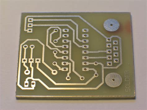
Board Layout: Once the schematic is complete, the PCB layout is created. This involves placing components on the board and routing the connections between them. The layout must consider factors such as signal integrity, power distribution, and manufacturability.
-
Design Rules: PCB design software includes design rules that help ensure the board meets manufacturing requirements. These rules include minimum trace widths, clearances, and hole sizes.
-
Signal Integrity: High-speed digital circuits require careful attention to signal integrity. This involves controlling impedance, minimizing crosstalk, and managing reflections.
-
EMI: Electronic devices must meet electromagnetic compatibility (EMC) requirements to avoid interfering with other devices. PCB design techniques such as proper grounding, shielding, and filtering can help minimize EMI.
-
Thermal Management: Power dissipation in electronic components can generate heat that must be managed to ensure reliable operation. PCB design techniques such as copper pours, thermal vias, and heatsinks can help dissipate heat.
PCB Design Software
There are several software tools available for PCB design. Some of the most popular include:
| Software | Vendor | Features |
|---|---|---|
| Altium Designer | Altium | Schematic capture, board layout, 3D modeling, simulation |
| OrCAD | Cadence | Schematic capture, board layout, simulation, design collaboration |
| EAGLE | Autodesk | Schematic capture, board layout, library management |
| KiCad | Open Source | Schematic capture, board layout, 3D modeling, simulation |
These software tools offer a range of features to help designers create high-quality PCBs efficiently.

PCB Fabrication
Once the PCB design is complete, the board must be fabricated. This involves several steps:
-
Gerber File Generation: The PCB design software generates Gerber files that describe the layers of the board, such as copper, solder mask, and silkscreen.
-
Board Fabrication: The Gerber files are sent to a PCB fabrication house, which uses them to create the physical board. This involves processes such as etching, drilling, and plating.
-
Assembly: After the board is fabricated, the components are soldered onto it. This can be done manually or using automated assembly machines.
-
Testing: The assembled board is tested to ensure it functions as intended. This can involve functional testing, in-circuit testing, and boundary scan testing.

PCB Design Considerations
When designing a PCB, there are several key considerations to keep in mind:
Component Selection
Selecting the right components is critical to the success of the design. Factors to consider include:
- Functionality: Does the component meet the requirements of the circuit?
- Availability: Is the component readily available from suppliers?
- Cost: Is the component cost-effective for the application?
- Footprint: Does the component have a standard footprint that can be easily incorporated into the PCB layout?
Board Stack-up
The board stack-up refers to the layers of the PCB and their arrangement. A typical stack-up might include:
- Top and bottom copper layers for signal routing
- Inner copper layers for power and ground planes
- Dielectric layers to insulate the copper layers
- Solder mask and silkscreen layers on the outer surfaces
The stack-up must be designed to meet the requirements of the circuit, such as impedance control and power distribution.
Signal Integrity
Signal integrity refers to the quality of the signals transmitted through the PCB. Factors that can affect signal integrity include:
- Impedance: The characteristic impedance of the traces must match the impedance of the source and load to avoid reflections.
- Crosstalk: Adjacent traces can capacitively couple, causing crosstalk that can corrupt signals.
- Electromagnetic Interference (EMI): High-frequency signals can radiate EMI that can interfere with other circuits or devices.
Techniques for managing signal integrity include:
- Controlled impedance: Using trace geometries and dielectric materials that provide the desired impedance.
- Differential signaling: Using differential pairs of traces to cancel out noise and EMI.
- Shielding: Using grounded copper planes or traces to shield sensitive signals.
Power Distribution
Power distribution is the process of delivering power to the components on the PCB. Factors to consider include:
- Voltage levels: The PCB may require multiple voltage levels for different components.
- Current requirements: The power distribution network must be able to supply the required current to each component.
- Decoupling: Decoupling capacitors must be placed close to the power pins of components to reduce noise and transients.
Techniques for managing power distribution include:
- Power and ground planes: Using dedicated copper layers for power and ground distribution.
- Via stitching: Using vias to connect the power and ground planes to the component pins.
- Decoupling capacitors: Placing decoupling capacitors close to the power pins of components.
Thermal Management
Thermal management is the process of dissipating heat generated by components on the PCB. Factors to consider include:
- Power dissipation: The amount of power dissipated by each component.
- Thermal resistance: The ability of the PCB and components to conduct heat.
- Ambient temperature: The temperature of the environment in which the PCB will operate.
Techniques for managing thermal issues include:
- Copper pours: Using large areas of copper to conduct heat away from components.
- Thermal vias: Using vias to conduct heat from the component to the copper layers.
- Heatsinks: Attaching heatsinks to high-power components to dissipate heat.

PCB Design Best Practices
To ensure a successful PCB design, there are several best practices to follow:
-
Start with a good schematic: The schematic is the foundation of the PCB design. Ensure that it is accurate, complete, and follows good design practices.
-
Use a grid: Using a grid helps to keep the layout organized and makes it easier to route traces.
-
Keep traces short: Shorter traces have lower resistance and inductance, which can improve signal integrity and reduce EMI.
-
Avoid right angles: Right-angle traces can cause reflections and EMI. Use 45-degree angles instead.
-
Use ground planes: Ground planes provide a low-impedance return path for signals and help to reduce EMI.
-
Decouple power supplies: Use decoupling capacitors close to the power pins of components to reduce noise and transients.
-
Control impedance: Use controlled impedance traces for high-speed signals to ensure signal integrity.
-
Simulate the design: Use simulation tools to verify the performance of the design before fabrication.
-
Follow design rules: Use design rules to ensure that the PCB can be manufactured reliably and cost-effectively.
-
Document the design: Create clear and complete documentation, including schematics, board layouts, and assembly drawings.
Frequently Asked Questions (FAQ)
-
What is the difference between a schematic and a PCB layout?
A schematic is a diagram that shows the electrical connections between components, while a PCB layout shows the physical placement of components on the board and the routing of traces between them. -
What is the purpose of a ground plane?
A ground plane is a large area of copper on a PCB layer that is connected to ground. It provides a low-impedance return path for signals and helps to reduce EMI. -
What is controlled impedance?
Controlled impedance is the practice of designing PCB traces to have a specific impedance, typically 50 ohms. This helps to ensure signal integrity and reduce reflections in high-speed circuits. -
What is a decoupling capacitor?
A decoupling capacitor is a capacitor placed close to the power pins of a component to reduce noise and transients on the power supply. -
What is the purpose of a solder mask?
A solder mask is a layer of insulating material applied to the outer layers of a PCB. It helps to prevent solder bridging and protects the copper traces from oxidation and damage.
Conclusion
PCB design is a critical step in the development of electronic devices. It involves creating a schematic, laying out the board, and considering factors such as signal integrity, power distribution, and thermal management. By following best practices and using the right tools and techniques, designers can create high-quality PCBs that are reliable, manufacturable, and cost-effective.
No responses yet