The Role of Software in Modern PCB Design
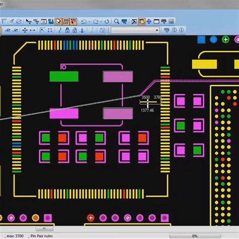
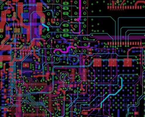
One of the most significant changes in PCB design has been the shift from manual drafting to computer-aided design (CAD) software. Modern PCB design software offers a range of powerful features that streamline the design process and enable engineers to create more complex and efficient designs.
Popular PCB Design Software
| Software | Manufacturer | Key Features |
|---|---|---|
| Altium Designer | Altium | 3D modeling, real-time collaboration, automated routing |
| Eagle | Autodesk | Schematic capture, PCB layout, library management |
| KiCad | Open Source | Schematic capture, PCB layout, 3D viewer, free |
| OrCAD | Cadence | Schematic capture, PCB layout, simulation, signal integrity analysis |
These software packages offer a range of benefits over traditional manual PCB design methods, including:
- Faster design iteration and prototyping
- Improved accuracy and precision
- Easier collaboration and version control
- Automated design rule checking (DRC) and error detection
- 3D visualization and modeling capabilities
The Impact of 3D Printing on PCB Prototyping
Another major development in the digital transformation of PCB design has been the rise of 3D printing technology. 3D printing allows designers to rapidly prototype PCBs and enclosures, reducing lead times and enabling faster iteration.
Benefits of 3D Printing for PCB Prototyping
- Rapid prototyping: 3D printing enables designers to quickly create physical prototypes of their PCBs, allowing for faster testing and iteration.
- Customization: 3D printing allows for greater customization of PCB shapes and sizes, as well as the creation of custom enclosures and housings.
- Cost-effectiveness: For low-volume prototypes, 3D printing can be more cost-effective than traditional manufacturing methods.
- Accessibility: 3D printers are becoming increasingly affordable and accessible, making it easier for designers to bring prototyping capabilities in-house.
However, it’s important to note that 3D printing is not a replacement for traditional PCB manufacturing methods, particularly for high-volume production runs. Instead, it serves as a valuable tool for rapid prototyping and design validation.
Cloud-Based Collaboration and Version Control
The digital transformation of PCB design has also enabled new forms of collaboration and version control. Cloud-based platforms allow teams to work together on designs in real-time, regardless of their physical location.
Popular Cloud-Based PCB Design Platforms
| Platform | Manufacturer | Key Features |
|---|---|---|
| Altium 365 | Altium | Real-time collaboration, version control, design reviews |
| Upverter | Altium | Browser-based design, real-time collaboration, version control |
| CircuitMaker | Altium | Free, community-driven design platform |
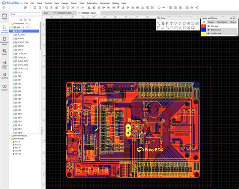
| EasyEDA | EasyEDA | Browser-based design, real-time collaboration, version control |
These platforms offer several benefits for PCB design teams, including:
- Real-time collaboration and communication
- Centralized version control and change tracking
- Secure access control and permissions management
- Integration with other tools and services (e.g., GitHub, Slack)
By leveraging cloud-based collaboration platforms, PCB design teams can work more efficiently, reduce errors and rework, and accelerate time-to-market.

Automated Design Rule Checking and Simulation
Another key aspect of the digital transformation in PCB design is the use of automated design rule checking (DRC) and simulation tools. These tools help designers catch errors early in the design process and validate the performance of their designs before physical prototyping.
Common DRC and Simulation Tools
| Tool | Manufacturer | Key Features |
|---|---|---|
| Cadence Allegro PCB Designer | Cadence | DRC, signal integrity analysis, thermal analysis |
| Mentor Graphics HyperLynx | Siemens EDA | Signal integrity analysis, power integrity analysis, EMI/EMC analysis |
| Ansys SIwave | Ansys | Signal integrity analysis, power integrity analysis, EMI/EMC analysis |
| Altium Designer | Altium | DRC, signal integrity analysis, 3D modeling |
DRC tools automatically check designs against a set of predefined rules, such as minimum trace widths, clearances, and hole sizes. This helps catch errors that might otherwise be missed by manual inspection.
Simulation tools, on the other hand, allow designers to analyze the electrical performance of their designs, including signal integrity, power integrity, and electromagnetic compatibility (EMC). By simulating the behavior of the PCB under various conditions, designers can identify and correct issues before committing to physical prototypes.
Intelligent Part Libraries and Supply Chain Integration
Digital transformation has also impacted the way PCB designers manage component libraries and interact with the supply chain. Intelligent part libraries and supply chain integration tools streamline the process of selecting and sourcing components for a design.
Benefits of Intelligent Part Libraries
- Centralized component data: Intelligent part libraries provide a single source of truth for component information, including datasheets, 3D models, and pricing data.
- Automated part selection: Some libraries can automatically recommend components based on design requirements, such as voltage, current, and package size.
- Real-time availability and pricing: Integration with distributor APIs allows designers to see real-time stock levels and pricing information for components.
- Supply chain risk management: Part libraries can flag components that are nearing end-of-life or have long lead times, helping designers make more informed decisions.
By leveraging intelligent part libraries and supply chain integration tools, PCB designers can reduce the time and effort required to select and source components, while also minimizing the risk of supply chain disruptions.
The Future of PCB Design: AI and Generative Design
Looking ahead, the digital transformation of PCB design is set to continue, driven by emerging technologies such as artificial intelligence (AI) and generative design.
AI in PCB Design
AI has the potential to revolutionize PCB design by automating many of the time-consuming and repetitive tasks involved in the design process. For example:
- Automated component placement and routing based on design constraints and performance requirements
- Intelligent design rule checking that learns from past designs and adapts to new requirements
- Predictive maintenance and failure analysis based on sensor data and machine learning models
Generative Design for PCBs
Generative design is another emerging technology that could transform the way PCBs are designed. In a generative design workflow, designers input their requirements and constraints, and the software generates a range of optimized designs that meet those criteria.
This approach has several potential benefits for PCB design, including:
- Faster exploration of the design space and identification of optimal solutions
- Improved performance and efficiency through the use of advanced optimization algorithms
- Reduced reliance on human expertise and intuition in the design process
While still in its early stages, generative design has the potential to significantly accelerate the PCB design process and enable the creation of more efficient and innovative designs.
Frequently Asked Questions (FAQ)
-
What is the most popular PCB design software?
Some of the most widely used PCB design software packages include Altium Designer, Autodesk Eagle, KiCad, and OrCAD. -
How does 3D printing benefit PCB prototyping?
3D printing enables rapid prototyping of PCBs and enclosures, allowing designers to quickly create physical prototypes for testing and iteration. It also enables greater customization and can be cost-effective for low-volume prototypes. -
What are the advantages of cloud-based collaboration for PCB design?
Cloud-based collaboration platforms allow PCB design teams to work together in real-time, regardless of their physical location. They also provide centralized version control, secure access management, and integration with other tools and services. -
How do automated design rule checking (DRC) tools work?
DRC tools automatically check PCB designs against a set of predefined rules, such as minimum trace widths, clearances, and hole sizes. This helps catch errors that might otherwise be missed by manual inspection. -
What is generative design, and how could it impact PCB design?
Generative design is an emerging technology that generates optimized designs based on user-defined requirements and constraints. In the context of PCB design, generative design could enable faster exploration of the design space, improved performance and efficiency, and reduced reliance on human expertise.
Conclusion
The digital transformation of PCB design is well underway, driven by advances in software, 3D printing, cloud-based collaboration, automation, and AI. These technologies are changing the way PCBs are designed, prototyped, and manufactured, enabling faster iteration, improved performance, and greater innovation.
As the digital transformation continues, it will be essential for PCB designers to stay up-to-date with the latest tools and techniques. By embracing new technologies and workflows, designers can create more efficient, reliable, and innovative PCBs that meet the evolving needs of the electronics industry.
No responses yet