Material Selection for RF PCBs
One of the most critical aspects of RF PCB design is the selection of appropriate materials. The substrate material and its properties significantly impact the performance of the circuit at high frequencies.
Substrate Materials
Common substrate materials used in RF PCBs include:
- FR-4: A popular choice for general-purpose PCBs, but its high dielectric loss and inconsistent performance at higher frequencies make it less suitable for RF applications.
- Rogers RO4000 Series: These high-frequency laminates offer excellent electrical properties, such as low dielectric loss and stable dielectric constant, making them ideal for RF PCBs.
- Teflon (PTFE): Known for its low dielectric loss and high thermal stability, Teflon is often used in demanding RF applications.
- Ceramic: Ceramic substrates, such as alumina and aluminum nitride, provide excellent thermal conductivity and low dielectric loss, making them suitable for high-power RF applications.
Copper Thickness and Surface Finish
The thickness and surface finish of the copper traces on an RF PCB also play a crucial role in its performance.
- Copper thickness: Thicker copper traces are generally preferred in RF PCBs to minimize resistive losses and improve power handling capacity. However, thicker traces can also increase the weight and cost of the PCB.
- Surface finish: The choice of surface finish can affect the signal integrity and solderability of the PCB. Common surface finishes for RF PCBs include Immersion Silver (ImAg), Electroless Nickel Immersion Gold (ENIG), and Hot Air Solder Leveling (HASL).
| Surface Finish | Advantages | Disadvantages |
|---|---|---|
| ImAg | Low cost, good solderability | Limited shelf life, prone to oxidation |
| ENIG | Excellent corrosion resistance, good solderability | Higher cost, potential for black pad formation |
| HASL | Low cost, good solderability | Uneven surface, potential for thermal shock |
RF PCB Layout and Design Considerations
Proper layout and design techniques are essential to minimize signal integrity issues and ensure optimal performance in RF PCBs.
Transmission Line Design
In RF PCBs, signals are often transmitted using controlled impedance transmission lines, such as microstrip and stripline.
- Microstrip: Consists of a single conductor trace on the top layer of the PCB, with a ground plane on the bottom layer. Microstrip is easier to fabricate and allows for easier component placement, but it is more susceptible to electromagnetic interference (EMI).
- Stripline: Consists of a conductor trace sandwiched between two ground planes. Stripline offers better EMI shielding and lower radiation losses compared to microstrip, but it is more challenging to fabricate and route.
Proper impedance matching and termination techniques should be employed to minimize reflections and signal distortions.
Ground Plane Design
A solid, uninterrupted ground plane is crucial for RF PCBs to provide a low-impedance return path for high-frequency signals and minimize EMI.
- Ground plane stitching: Use multiple vias to connect ground planes on different layers, minimizing impedance differences and ensuring a consistent reference plane.
- Avoid split ground planes: Splitting the ground plane can create unwanted resonances and degrade signal integrity.
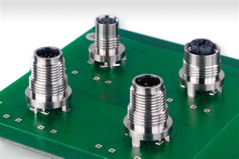
Component Placement and Routing
Careful component placement and routing techniques can help minimize parasitics and reduce signal interference.
- Keep RF traces short: Minimize the length of RF traces to reduce losses and avoid unwanted radiations.
- Avoid sharp bends: Use smooth, gradual bends in RF traces to minimize reflections and impedance discontinuities.
- Component orientation: Orient components to minimize coupling and cross-talk between adjacent traces.
- Decoupling capacitors: Place decoupling capacitors close to active components to minimize power supply noise and improve signal integrity.

RF PCB Manufacturing Considerations
The manufacturing process for RF PCBs requires special attention to ensure consistent performance and reliability.
Tight Tolerances
RF PCBs often require tighter manufacturing tolerances compared to general-purpose PCBs.
- Trace width and spacing: Maintain precise trace widths and spacing to ensure consistent impedance and minimize cross-talk.
- Dielectric thickness: Control the thickness of the dielectric material to maintain consistent impedance and minimize variations in signal propagation.
Multilayer PCBs
Multilayer RF PCBs can help minimize the PCB size and improve signal routing, but they require careful layer stackup design.
- Layer stackup: Optimize the layer stackup to minimize crosstalk and ensure proper impedance control.
- Blind and buried vias: Use blind and buried vias to minimize the PCB size and improve signal routing, but be aware of the increased manufacturing complexity and cost.
Quality Control and Testing
Stringent quality control and testing procedures should be implemented to ensure the performance and reliability of RF PCBs.
- Visual inspection: Perform visual inspections to check for manufacturing defects, such as shorts, opens, and incorrect component placement.
- Electrical testing: Conduct electrical tests, such as time-domain reflectometry (TDR) and vector network analyzer (VNA) measurements, to verify signal integrity and impedance matching.
- Environmental testing: Perform environmental tests, such as thermal cycling and humidity exposure, to ensure the PCB’s reliability under various operating conditions.

RF PCB Assembly and Soldering
The assembly and soldering process for RF PCBs requires special care to minimize signal degradation and ensure reliable connections.
Soldering Techniques
Use appropriate soldering techniques to minimize thermal stress and ensure reliable connections.
- Hand soldering: For low-volume production or prototyping, hand soldering can be used, but it requires skilled operators to ensure consistent results.
- Reflow soldering: For high-volume production, reflow soldering is preferred, as it provides consistent and reliable results. However, proper thermal profiling is essential to avoid component damage.
Cleaning and Conformal Coating
After soldering, RF PCBs should be thoroughly cleaned to remove flux residues and other contaminants that can degrade signal integrity.
- Cleaning agents: Use appropriate cleaning agents, such as isopropyl alcohol or specialized PCB cleaners, to remove flux residues and other contaminants.
- Conformal coating: Apply a conformal coating to protect the PCB from moisture, dust, and other environmental factors that can affect its performance and reliability.

Frequently Asked Questions (FAQ)
- What is the difference between an RF PCB and a general-purpose PCB?
-
RF PCBs are designed to handle high-frequency signals and require specialized materials, layout techniques, and manufacturing processes to ensure optimal performance and signal integrity. General-purpose PCBs, on the other hand, are designed for lower-frequency applications and have less stringent requirements.
-
What are the most common substrate materials used in RF PCBs?
-
Common substrate materials for RF PCBs include Rogers RO4000 series, Teflon (PTFE), and ceramic materials such as alumina and aluminum nitride. These materials offer low dielectric loss, stable dielectric constant, and good thermal properties, making them suitable for high-frequency applications.
-
Why is a solid ground plane important in RF PCB design?
-
A solid, uninterrupted ground plane is crucial in RF PCBs to provide a low-impedance return path for high-frequency signals and minimize electromagnetic interference (EMI). It helps maintain signal integrity and reduces unwanted radiations.
-
What are the advantages of using blind and buried vias in RF PCBs?
-
Blind and buried vias can help minimize the PCB size and improve signal routing in multilayer RF PCBs. They allow for more efficient use of board space and can reduce the overall length of RF traces, minimizing losses and unwanted radiations. However, they also increase the manufacturing complexity and cost.
-
Why is thorough cleaning important after soldering RF PCBs?
- Thorough cleaning of RF PCBs after soldering is essential to remove flux residues and other contaminants that can degrade signal integrity and affect the PCB’s performance. Cleaning helps ensure reliable connections and maintains the PCB’s long-term reliability.
In conclusion, designing and manufacturing RF PCBs requires careful consideration of various factors, including material selection, layout and design techniques, manufacturing processes, assembly, and soldering. By addressing these key aspects and following best practices, engineers can ensure optimal performance, signal integrity, and reliability in their RF PCB designs.
No responses yet