Introduction to PCBs and HDI Technology
Printed Circuit Boards (PCBs) are the backbone of modern electronics. These boards mechanically support and electrically connect electronic components using conductive tracks, pads and other features etched from copper sheets laminated onto a non-conductive substrate. PCBs are used in virtually all electronic products including computers, smartphones, appliances, medical devices, aerospace systems, and much more.
As electronics continue to get smaller, more complex and pack in more functionality, the demands on PCB technology keep increasing. This is where High Density Interconnect (HDI) PCBs come into play. HDI is a leading-edge PCB manufacturing technology that enables the production of boards with finer lines and spaces, smaller vias, higher connection pad density, and higher connection density per unit area compared to traditional PCB fabrication techniques.
HDI PCBs offer many advantages that make them the perfect choice for a wide range of advanced electronics applications. This article will take an in-depth look at what HDI technology is, the benefits it provides, and why it has become an essential enabling technology for next-generation electronic products and systems.
What is HDI PCB Technology?
HDI, which stands for High Density Interconnect, is a PCB manufacturing technology that involves the fabrication of very fine circuit traces and interconnections. The official definition of HDI is constantly evolving as PCB fabrication capabilities advance, but in general an HDI PCB is one that has:
- Higher wiring density per unit area (>20 in/cm2)
- Finer lines and spaces (<100 μm)
- Smaller via diameters (<150 μm)
- Higher connection pad density (>20 pads/cm2)
- Sequential lamination construction with multiple layers of micro vias
Essentially, HDI lets PCB designers create smaller, denser interconnects between components. This increased interconnect density is achieved through the use of blind and buried vias and the stacking or sequential lamination of multiple HDI layers.
Types of HDI PCBs
There are three main types or classifications of HDI PCBs:
| Type | Description |
|---|---|
| 1 | Single-sided HDI – Has one HDI layer with through vias and microvias |
| 2 | Double-sided HDI – HDI layers on both sides with through vias |
| 3 | Multi-layer HDI – 3 or more HDI layers with stacked micro vias |
The different HDI types support various levels of design complexity and interconnect density. Type 3 HDI is the most advanced and allows for the highest wiring density currently possible.
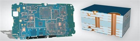
HDI PCB Stack-ups
The stack-up refers to the arrangement of copper and insulating layers that make up a PCB. HDI stack-ups involve multiple layers of microvias (blind and/or buried vias with diameters <150 μm) that interconnect the high density circuitry on the outer layers.
Some common HDI stack-ups include:
- 1-N-1 (Type 1): 1 HDI layer, N core layers, 1 HDI layer
- 2-N-2 (Type 2): 2 HDI layers, N core layers, 2 HDI layers
- 3-N-3 (Type 3): 3 HDI layers, N core layers, 3 HDI layers
- i-N-i (Type 3): i HDI layers, N core layers, i HDI layers (i > 3)
The number of HDI layers and the type of vias used will depend on the complexity and density requirements of the PCB design. More complex HDI stack-ups enable higher interconnect densities but are also more challenging and costly to manufacture.

Benefits and Advantages of HDI PCBs
HDI PCBs offer a range of important benefits for electronic products and systems. Some of the key advantages include:
1. Miniaturization
One of the biggest benefits of HDI is that it enables the miniaturization of electronic devices. By providing a way to increase the density of interconnects, HDI allows more functionality to be packed into a smaller form factor. Products can be made thinner, lighter, and more compact overall.
2. Improved Electrical Performance
The denser interconnects and shorter signal paths enabled by HDI improve electrical performance in several ways. With shorter paths between components, signal integrity is better maintained. Additionally, the lower impedance of the finer traces decreases electromagnetic interference (EMI). The transition to microvias also helps reduce signal attenuation and EMI.
3. Reduced Power Consumption
The shorter interconnects enabled by HDI help lower power consumption in two ways. First, signals traveling shorter distances encounter less resistance, so less energy is dissipated as heat. Second, not as large a voltage is needed to send signals over shorter paths, further reducing power needs.
4. Enhanced Reliability
HDI PCBs are known for their high reliability, even in harsh operating conditions. A big reason for this is the use of microvias which create strong mechanical connections between layers. Microvias are also less prone to misregistration and breakage than larger through-hole vias. Additionally, HDI substrates and coatings are selected to withstand extreme temperatures, shocks and vibrations.
5. Design Flexibility
HDI opens up new possibilities for PCB designers by providing the ability to route more connections in a smaller space. The use of blind and buried vias frees up space on the outer layers for components. More design flexibility is also achieved by varying the microvia and trace dimensions on different layers to meet signal integrity and EMI requirements.
6. Cost Reduction
While HDI boards have a higher cost per unit area than conventional PCBs, they can reduce costs at the system level. By enabling higher component density, HDI allows more functionality to be fit onto a smaller board. This can decrease the number of boards and interconnections required, simplifying assembly and lowering overall system costs. The improved reliability of HDI also helps reduce repair and maintenance expenses over the life of a product.

Applications of HDI PCB Technology
The benefits of HDI make it a key enabling technology for electronics across a wide range of industries and applications. Some of the most common uses of HDI include:
Consumer Electronics
HDI is used extensively in smartphones, tablets, laptops, wearables and other compact, high-performance consumer electronics. The miniaturization and enhanced functionality enabled by HDI are essential for meeting consumer demand for more advanced, pocketable devices.
Telecommunications
In telecom applications like network switches and routers, HDI helps meet requirements for higher bandwidth, faster data speeds and lower latency. 5G wireless infrastructure, Internet of Things (IoT) devices, and optical communication modules are some of the telecom applications driving HDI adoption.
Automotive
From infotainment systems to advanced driver assistance systems (ADAS) and autonomous driving, vehicles are incorporating a rapidly growing amount of electronics. HDI is used to create the compact, high-reliability control modules, sensors and displays these complex systems require.
Aerospace and Defense
Aerospace and defense applications demand the highest levels of performance and reliability in extreme environmental conditions. HDI is used to create mission-critical systems like avionics, navigation, radar, and satellite communications that meet strict size, weight and power (SWaP) constraints.
Medical Devices
Medical electronic devices like wearable health monitors, implants, imaging systems and surgical robotics are shrinking in size while growing in capability. HDI allows the miniaturization and high connection densities needed for these increasingly small yet sophisticated devices.
Industrial Automation
HDI is being adopted in industrial automation for machine vision systems, robotics, process control, and data acquisition. The compact, ruggedized electronics enabled by HDI help improve efficiency and reliability on the factory floor.

HDI PCB Design Considerations
Designing HDI PCBs involves different constraints and tradeoffs than traditional PCB design. Here are some of the key considerations:
1. Component Selection
The component size, pitch and density are important factors in HDI design. Smaller passive components and fine-pitch BGAs and CSPs are typically used to take full advantage of HDI’s denser interconnects. Designers must balance component selections with availability and cost.
2. Layer Stack-up
The layer stack-up is critical for meeting signal integrity, power distribution and EMI requirements in an HDI design. Factors like the number of HDI layers, microvia layout, trace widths/spacing, and dielectric thicknesses must be carefully optimized.
3. Via Types and Placement
HDI designs use blind, buried and micro via structures to maximize interconnect density. The type, size and placement of vias must be properly planned to ensure manufacturability and reliability. Staggered and stacked micro vias are used to connect multiple HDI layers.
4. Signal Integrity
Maintaining signal integrity is paramount in HDI designs with their denser traces and closer spacing. Signal crossing, crosstalk and electromagnetic interference (EMI) must be minimized through proper trace routing, impedance control, and shielding techniques.
5. Power Integrity
Proper power distribution is essential for maintaining signal integrity and minimizing EMI in HDI PCBs. The use of power planes, decoupling capacitors, and careful placement of power and ground pins are important considerations.
6. Design for Manufacturing (DFM)
Designing for manufacturability is critical for HDI PCBs. The tight tolerances and small features can make HDI designs more prone to manufacturing defects. Following the PCB manufacturer’s DFM guidelines for minimum trace width/spacing, via sizes, and drilled hole-to-copper clearances will help ensure a successful, high-yield fabrication process.
Frequently Asked Questions (FAQ)
1. What is the difference between HDI PCBs and regular PCBs?
HDI PCBs have much finer lines and spaces (<100 μm), smaller vias (<150 μm), and higher interconnect densities (>20 in/cm2) compared to regular PCBs. HDI PCBs also use blind and buried vias and sequential lamination of multiple high density layers, whereas regular PCBs typically only have through-hole vias and a single lamination cycle.
2. Are HDI PCBs more expensive?
Yes, HDI PCBs are more expensive per unit area than regular PCBs due to their greater complexity, tighter tolerances, and additional manufacturing steps. However, HDI can reduce overall system costs by allowing more functionality to be fit into a smaller space, reducing the number of boards and interconnects required.
3. What industries use HDI PCBs?
HDI PCBs are used in a wide range of industries including consumer electronics, telecommunications, automotive, aerospace, defense, medical devices, and industrial automation. Basically any application that requires high interconnect density, miniaturization, and high performance can benefit from HDI.
4. What are the key design considerations for HDI PCBs?
Some of the most important design considerations for HDI PCBs include component selection, layer stack-up, via types and placement, signal and power integrity, and design for manufacturing (DFM). HDI designs must carefully balance these different factors to meet performance, reliability and cost requirements.
5. What is the future outlook for HDI technology?
The demand for HDI PCBs is expected to continue growing rapidly as electronics become increasingly miniaturized and sophisticated across all industries. Advancements in materials, processes and design tools will enable even finer features and higher interconnect densities in the future. Some emerging trends in HDI include substrate-like PCBs, any-layer HDI, and embedded active and passive components.
Conclusion
In conclusion, HDI PCBs are a critical enabling technology for advanced electronics across a wide range of industries and applications. By providing a way to dramatically increase interconnect density compared to traditional PCBs, HDI allows greater functionality to be packed into smaller, higher-performance products.
The benefits of HDI – including miniaturization, improved electrical performance, lower power consumption, higher reliability, increased design flexibility, and cost reduction at the system level – make it the perfect choice to meet the demanding size, weight and performance requirements of next-generation electronic devices and systems.
As HDI technology continues to evolve, it will play an increasingly vital role in shaping the future of electronics. Designers who understand how to leverage HDI in their products will be well-positioned to create the breakthrough innovations that define the electronic landscape in the years ahead.
No responses yet