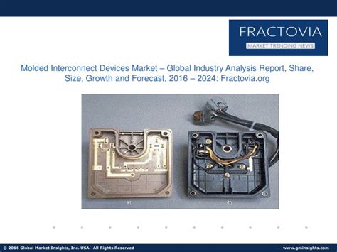
What are Molded Interconnect Devices?
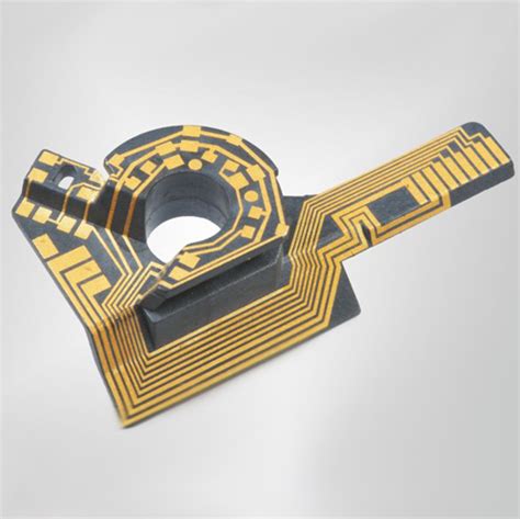
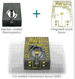
Molded Interconnect Devices are three-dimensional (3D) injection-molded thermoplastic parts with integrated electrical circuits. The circuits are created by selectively metallizing the surface of the molded plastic substrate, allowing for the integration of both electrical and mechanical functions into a single component. This process eliminates the need for separate PCBs and mechanical parts, resulting in a more compact, lightweight, and cost-effective solution.
The MID manufacturing process typically involves the following steps:
- Injection molding of the thermoplastic substrate
- Laser direct structuring (LDS) or two-shot molding to create the desired circuit pattern
- Metallization of the circuit pattern using electroless plating or other plating techniques
- Component assembly and final testing
Advantages of Molded Interconnect Devices
MIDs offer several key advantages over traditional PCBs and separate mechanical components:
-
Miniaturization: MIDs allow for the integration of electrical and mechanical functions into a single, compact component, reducing the overall size and weight of the final product.
-
Cost reduction: By eliminating the need for separate PCBs and mechanical parts, MIDs can significantly reduce manufacturing and assembly costs.
-
Improved reliability: The integrated nature of MIDs reduces the number of interconnections and solder joints, resulting in improved reliability and reduced risk of failure.
-
Design flexibility: MIDs enable the creation of complex, three-dimensional structures that would be difficult or impossible to achieve with traditional PCBs.
-
Enhanced performance: The 3D structure of MIDs allows for shorter signal paths and improved shielding, resulting in better electrical performance and reduced electromagnetic interference (EMI).
Applications of Molded Interconnect Devices
MIDs have found applications in various industries, including:
Automotive
In the automotive industry, MIDs are used for a wide range of applications, such as:
- Sensors (e.g., pressure, temperature, and humidity sensors)
- Lighting systems (e.g., LED headlights and taillights)
- Antennas (e.g., GPS, radio, and cellular antennas)
- Switches and control panels
MIDs offer significant benefits in automotive applications, including reduced weight, improved reliability, and enhanced performance in harsh environments.
Medical
MIDs are increasingly being used in medical devices, such as:
- Hearing aids
- Pacemakers
- Insulin pumps
- Surgical instruments
The compact size, improved reliability, and design flexibility of MIDs make them well-suited for medical applications, where miniaturization and reliability are critical.
Consumer Electronics
MIDs are used in a variety of consumer electronics products, including:
- Smartphones and tablets
- Wearable devices (e.g., smartwatches and fitness trackers)
- Gaming controllers
- Virtual and augmented reality headsets
In these applications, MIDs enable the creation of lightweight, compact, and feature-rich devices that meet the demands of today’s consumers.
MID Manufacturing Processes
There are two primary methods for creating the circuit patterns on MIDs: laser direct structuring (LDS) and two-shot molding.
Laser Direct Structuring (LDS)
Laser direct structuring is the most common method for creating circuit patterns on MIDs. In this process, a thermoplastic substrate containing a special additive is injection molded into the desired shape. A laser is then used to selectively activate the additive in the areas where the circuit pattern will be formed. The activated areas are then metallized using electroless plating, creating the final circuit pattern.
Advantages of LDS include:
- Design flexibility: LDS allows for the creation of complex, high-resolution circuit patterns on 3D surfaces.
- Scalability: The LDS process is well-suited for high-volume production.
- Material compatibility: LDS is compatible with a wide range of thermoplastic materials, including polyamide (PA), liquid crystal polymer (LCP), and polyphthalamide (PPA).
Two-Shot Molding
In the two-shot molding process, two different thermoplastic materials are injection molded in sequence to create the MID substrate. The first shot molds the base substrate using a non-platable material, while the second shot molds the circuit pattern using a platable material. The platable areas are then metallized using electroless plating or other plating techniques.
Advantages of two-shot molding include:
- Material flexibility: Two-shot molding allows for the use of a wider range of thermoplastic materials, as the platable and non-platable areas can be made from different materials.
- Simplified process: Two-shot molding eliminates the need for laser activation, simplifying the overall manufacturing process.

Design Considerations for Molded Interconnect Devices
When designing MIDs, several key factors must be considered to ensure optimal performance and manufacturability:
Material Selection
The choice of thermoplastic material for the MID substrate is critical, as it must meet the mechanical, thermal, and electrical requirements of the application. Common materials used for MIDs include polyamide (PA), liquid crystal polymer (LCP), and polyphthalamide (PPA). The material must also be compatible with the chosen manufacturing process (LDS or two-shot molding).
Circuit Design
The circuit design for MIDs must take into account the 3D nature of the substrate and the limitations of the manufacturing process. Key considerations include:
- Minimum feature size: The minimum width and spacing of the circuit traces must be compatible with the resolution of the manufacturing process.
- Circuit layout: The circuit layout must be optimized for the 3D structure of the MID, considering factors such as signal path length, impedance matching, and EMI shielding.
- Component placement: The placement of components on the MID substrate must consider the mechanical and thermal requirements of the application, as well as the accessibility for assembly and testing.
Mechanical Design
The mechanical design of the MID substrate must consider the functional requirements of the application, as well as the limitations of the injection molding process. Key factors include:
- Wall thickness: The wall thickness of the MID substrate must be uniform and appropriate for the chosen material and manufacturing process.
- Draft angles: Adequate draft angles must be incorporated into the design to ensure proper ejection from the injection mold.
- Structural features: Ribs, bosses, and other structural features must be designed to provide the necessary mechanical strength and stability while minimizing warpage and other molding defects.
Future Trends in Molded Interconnect Devices
As the demand for smaller, lighter, and more integrated electronic devices continues to grow, the use of MIDs is expected to increase in the coming years. Some of the key trends and developments in MID technology include:
-
Advanced materials: The development of new thermoplastic materials with improved mechanical, thermal, and electrical properties will expand the range of applications for MIDs.
-
Multi-layer MIDs: The development of multi-layer MID technology, which allows for the creation of more complex circuit patterns and higher component densities, will enable the design of even more compact and sophisticated devices.
-
Hybrid MIDs: The combination of MIDs with other technologies, such as printed electronics and embedded components, will lead to the creation of hybrid devices with enhanced functionality and performance.
-
Sustainable manufacturing: As environmental concerns continue to drive innovation in manufacturing, the development of more sustainable MID materials and processes, such as biodegradable plastics and low-energy metallization techniques, will become increasingly important.
Frequently Asked Questions (FAQ)
-
Q: What are the main advantages of MIDs over traditional PCBs?
A: MIDs offer several advantages over traditional PCBs, including reduced size and weight, improved reliability, design flexibility, and enhanced electrical performance. By integrating electrical and mechanical functions into a single component, MIDs can also significantly reduce manufacturing and assembly costs. -
Q: What are the most common materials used for MID substrates?
A: The most common materials used for MID substrates are thermoplastics, such as polyamide (PA), liquid crystal polymer (LCP), and polyphthalamide (PPA). These materials offer a combination of good mechanical, thermal, and electrical properties, as well as compatibility with the MID manufacturing processes. -
Q: What are the two main manufacturing processes for creating circuit patterns on MIDs?
A: The two main manufacturing processes for creating circuit patterns on MIDs are laser direct structuring (LDS) and two-shot molding. LDS uses a laser to selectively activate areas of the substrate for metallization, while two-shot molding involves the sequential injection molding of platable and non-platable materials to create the circuit pattern. -
Q: What are some of the key applications for MIDs in the automotive industry?
A: In the automotive industry, MIDs are used for a wide range of applications, including sensors (e.g., pressure, temperature, and humidity sensors), lighting systems (e.g., LED headlights and taillights), antennas (e.g., GPS, radio, and cellular antennas), and switches and control panels. MIDs offer benefits such as reduced weight, improved reliability, and enhanced performance in harsh environments. -
Q: What are some of the future trends in MID technology?
A: Some of the key future trends in MID technology include the development of advanced materials with improved properties, the creation of multi-layer MIDs for more complex circuit patterns and higher component densities, the combination of MIDs with other technologies to create hybrid devices, and the development of more sustainable MID materials and manufacturing processes.
No responses yet