Table of Contents
- Introduction to Wave Soldering
- Wave Soldering Process
- Pre-heating
- Fluxing
- Solder Wave
- Cooling
- Advantages of Wave Soldering
- Challenges in Wave Soldering
- Thermal Stress
- Bridging and Icicles
- Insufficient Wetting
- Solder Balling
- Wave Soldering Equipment
- Conveyor System
- Fluxer
- Solder Pot and Wave
- Heaters
- Process Parameters and Optimization
- Solder Alloy Selection
- Flux Selection
- Preheat Temperature
- Conveyor Speed
- Solder Wave Height and Angle
- PCB Design Considerations for Wave Soldering
- Component Placement
- Solder Mask and Pad Design
- Thermal Relief
- Troubleshooting Common Wave Soldering Defects
- Bridging
- Insufficient Fillets
- Solder Balls
- Lifted Components
- Quality Control and Inspection
- Visual Inspection
- Automated Optical Inspection (AOI)
- X-ray Inspection
- Environmental and Safety Considerations
- Frequently Asked Questions (FAQ)
- Conclusion
Introduction to Wave Soldering
Wave soldering is an automated process that involves passing a printed circuit board (PCB) over a molten solder wave to create electrical connections between the components and the board. This technique is particularly suitable for through-hole components and is widely used in the electronics industry for its efficiency and reliability in mass production.
The wave soldering process consists of several key steps: pre-heating, fluxing, soldering, and cooling. Each step plays a crucial role in ensuring the quality and integrity of the solder joints. By understanding the principles behind wave soldering and optimizing the process parameters, manufacturers can achieve consistent and reliable results, minimizing defects and improving overall product quality.

Wave Soldering Process
The wave soldering process involves a series of steps that work together to create a reliable solder joint between the components and the PCB. Let’s take a closer look at each step:
Pre-heating
Before the PCB enters the solder wave, it passes through a pre-heating zone. The purpose of pre-heating is to gradually raise the temperature of the board and components, minimizing thermal shock and reducing the risk of component damage. Pre-heating also activates the flux and improves the wetting of the solder.
The ideal pre-heating temperature depends on the type of PCB, components, and solder alloy used. Typically, the pre-heating temperature ranges from 80°C to 150°C, with a specific ramp-up rate to avoid thermal stress.
Fluxing
After pre-heating, the PCB moves to the fluxing stage. Flux is a chemical compound that removes oxides from the metal surfaces, promoting better wetting and adhesion of the solder. The flux is applied to the bottom side of the PCB, either through a spray or foam fluxing system.
The choice of flux depends on the type of PCB, components, and solder alloy. There are various types of fluxes available, including rosin-based, water-soluble, and no-clean fluxes, each with its own advantages and limitations.
Solder Wave
Once the PCB is pre-heated and fluxed, it enters the solder wave. The solder wave is created by pumping molten solder through a nozzle, forming a standing wave that contacts the bottom side of the PCB. As the board moves over the wave, the molten solder wets the component leads and PCB pads, creating a strong mechanical and electrical connection.
The solder wave is typically composed of a tin-lead alloy, although lead-free alloys are becoming increasingly common due to environmental and health concerns. The temperature of the solder wave is carefully controlled, usually between 240°C and 260°C, to ensure optimal fluidity and wetting properties.
Cooling
After the PCB exits the solder wave, it enters a cooling zone. The cooling process allows the molten solder to solidify, forming a strong and reliable joint. Cooling can be achieved through natural convection, forced air, or a combination of both.
Proper cooling is essential to prevent thermal shock and ensure the formation of a fine-grained solder structure, which contributes to the mechanical strength and reliability of the joint.

Advantages of Wave Soldering
Wave soldering offers several key advantages over other soldering techniques, making it a popular choice for mass production in the electronics industry:
-
High Throughput: Wave soldering is an automated process that allows for the rapid soldering of multiple PCBs in succession, enabling high production rates and reduced cycle times.
-
Consistency: The automated nature of wave soldering ensures consistent solder joint quality across a large number of PCBs, reducing the risk of human error associated with manual soldering.
-
Cost-effectiveness: Wave soldering is a cost-effective solution for mass production, as it reduces labor costs and minimizes the need for rework and repairs.
-
Versatility: Wave soldering can accommodate a wide range of PCB sizes, shapes, and component types, making it suitable for various applications and industries.
-
Reliability: When properly optimized, wave soldering produces strong, reliable solder joints that can withstand mechanical stress and environmental factors, ensuring the long-term performance of the electronic device.

Challenges in Wave Soldering
Despite its numerous advantages, wave soldering also presents some challenges that manufacturers must address to ensure optimal results. Some of the most common challenges include:
Thermal Stress
During wave soldering, the PCB and components are subjected to rapid temperature changes, which can lead to thermal stress. Thermal stress can cause component damage, board warpage, and solder joint defects. To minimize thermal stress, it is essential to carefully control the pre-heating and cooling rates, as well as the solder wave temperature.
Bridging and Icicles
Bridging occurs when excess solder accumulates between adjacent pins or pads, creating an unintended electrical connection. Icicles, on the other hand, are sharp, needle-like projections of solder that can cause short circuits or mechanical damage. These defects can be minimized by optimizing the solder wave height, angle, and conveyor speed, as well as ensuring proper PCB design and component placement.
Insufficient Wetting
Insufficient wetting occurs when the molten solder fails to adhere properly to the component leads or PCB pads, resulting in weak or incomplete solder joints. This can be caused by factors such as poor fluxing, incorrect solder temperature, or contaminated surfaces. Ensuring proper fluxing, maintaining the optimal solder temperature, and keeping the PCB and components clean can help prevent insufficient wetting.
Solder Balling
Solder balling refers to the formation of small, spherical solder particles on the PCB surface or component leads. These balls can cause short circuits or interfere with the proper functioning of the device. Solder balling can be caused by factors such as excessive solder wave height, incorrect flux application, or contaminated surfaces. Optimizing the wave soldering parameters and maintaining a clean environment can help minimize solder balling.
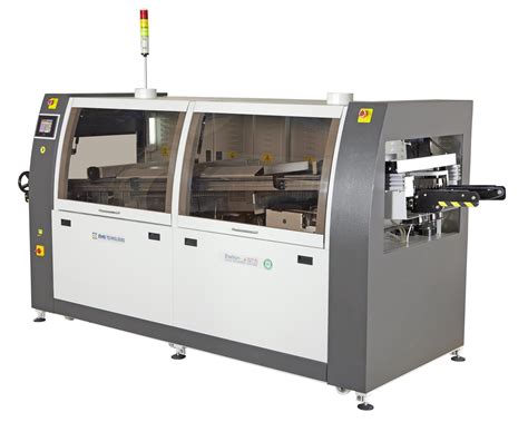
Wave Soldering Equipment
To perform wave soldering effectively, several key pieces of equipment are required. Let’s take a closer look at each of these components:
Conveyor System
The conveyor system is responsible for transporting the PCBs through the various stages of the wave soldering process. It consists of a series of rails, belts, or chains that move the boards at a controlled speed, ensuring consistent exposure to the pre-heating, fluxing, and soldering zones. The conveyor speed is a critical parameter that affects the quality of the solder joints and must be carefully optimized based on the specific requirements of the PCB and components.
Fluxer
The fluxer is responsible for applying flux to the bottom side of the PCB before it enters the solder wave. Flux is essential for removing oxides from the metal surfaces and promoting better wetting and adhesion of the solder. There are two main types of fluxers: spray fluxers and foam fluxers.
Spray fluxers use a pressurized spray system to apply a fine mist of flux to the PCB surface. They offer precise control over the flux application and are suitable for a wide range of flux types and PCB designs.
Foam fluxers, on the other hand, use a foam-generating system to create a stable foam layer on the surface of the flux reservoir. As the PCB passes over the foam, the flux is applied evenly to the bottom side. Foam fluxers are known for their simplicity and cost-effectiveness.
Solder Pot and Wave
The solder pot is a reservoir that holds the molten solder alloy. It is typically made of a heat-resistant material, such as ceramic or graphite, and is equipped with heating elements to maintain the solder at the desired temperature.
The solder wave is created by pumping the molten solder from the pot through a nozzle or series of nozzles. The design of the wave nozzle is crucial for achieving the optimal wave shape and flow characteristics. Common wave nozzle designs include the lambda wave, chip wave, and turbulent wave, each offering specific advantages for different PCB and component types.
Heaters
Heaters are used in the pre-heating and soldering zones to maintain the desired temperature profile throughout the wave soldering process. There are several types of heaters commonly used in wave soldering machines:
-
Infrared (IR) Heaters: IR heaters use radiant energy to heat the PCB and components. They offer fast response times and precise temperature control, making them suitable for a wide range of applications.
-
Convection Heaters: Convection heaters use hot air to heat the PCB and components. They provide uniform heating and are particularly effective for PCBs with high thermal mass or densely populated boards.
-
Quartz Heaters: Quartz heaters use quartz lamps to generate intense, focused heat. They are often used in the pre-heating stage to quickly raise the temperature of the PCB and components.
The choice of heaters depends on factors such as the PCB design, component types, and desired temperature profile. In many cases, a combination of different heater types is used to achieve the optimal heating performance.
Process Parameters and Optimization
To achieve the best results in wave soldering, several key process parameters must be carefully controlled and optimized. These parameters include:
Solder Alloy Selection
The choice of solder alloy is critical for achieving strong, reliable solder joints. The most common solder alloys used in wave soldering are tin-lead (SnPb) and lead-free alloys, such as tin-silver-copper (SAC).
Tin-lead alloys, typically Sn63Pb37, have been widely used in the electronics industry due to their excellent wetting properties, low melting point, and good mechanical strength. However, due to environmental and health concerns, the use of lead-based alloys has been restricted by various regulations, such as the Restriction of Hazardous Substances (RoHS) directive.
Lead-free alloys, such as SAC305 (Sn96.5Ag3.0Cu0.5), have become increasingly popular as a substitute for tin-lead alloys. These alloys offer good mechanical strength and reliability, but they require higher soldering temperatures and may present challenges in terms of wetting and joint formation.
The selection of the solder alloy depends on factors such as the PCB design, component compatibility, environmental requirements, and cost considerations.
Flux Selection
The choice of flux is another critical factor in wave soldering. Flux is responsible for removing oxides from the metal surfaces, promoting better wetting and adhesion of the solder. There are several types of fluxes available, each with its own advantages and limitations:
-
Rosin-based Fluxes: Rosin-based fluxes are derived from pine tree resins and are available in various activity levels, from mild to highly activated. They offer good wetting properties and are suitable for a wide range of applications. However, rosin-based fluxes require cleaning after soldering to remove residues that can cause corrosion or affect the long-term reliability of the solder joints.
-
Water-soluble Fluxes: Water-soluble fluxes are designed to be easily removed with water after soldering. They offer excellent wetting properties and are suitable for applications where cleanliness is critical. However, water-soluble fluxes can be more corrosive than rosin-based fluxes and may require stricter process control to prevent excessive activation.
-
No-clean Fluxes: No-clean fluxes are formulated to leave minimal, non-corrosive residues after soldering, eliminating the need for post-soldering cleaning. They are popular in applications where cleaning is impractical or cost-prohibitive. However, no-clean fluxes may have lower activity levels compared to other flux types, which can affect wetting and joint formation in some cases.
The selection of flux depends on factors such as the PCB design, component types, soldering requirements, and environmental considerations.
Preheat Temperature
The preheat temperature is a critical parameter in wave soldering, as it affects the wetting properties of the solder and the thermal stress on the components. The ideal preheat temperature depends on the type of PCB, components, and solder alloy used.
For tin-lead solders, the typical preheat temperature range is 80°C to 120°C, while for lead-free solders, the range is 100°C to 150°C. The preheat temperature should be carefully controlled to ensure that the PCB and components reach the desired temperature uniformly, without causing thermal shock or damage.
Insufficient preheating can result in poor wetting and incomplete solder joint formation, while excessive preheating can cause component damage, board warpage, and increased oxidation of the metal surfaces.
Conveyor Speed
The conveyor speed determines the time that the PCB spends in contact with the solder wave, which affects the quality of the solder joints. A slower conveyor speed allows for longer contact time, promoting better wetting and filling of the through-holes. However, excessive contact time can lead to overheating of the components and increased risk of defects, such as bridging or icicles.
On
No responses yet