Introduction to Voltage Boosting Circuits
A voltage boosting circuit, also known as a Boost Converter or step-up converter, is an electronic circuit that increases the voltage from a DC power source to a higher DC voltage level. Voltage boosting circuits are commonly used in applications where a higher voltage is needed than what the power source can directly supply, such as in battery-powered devices, solar power systems, and LED drivers.
The basic principle behind a voltage boosting circuit is to store energy in an inductor when a switch is closed, and then release that energy at a higher voltage when the switch opens. By rapidly opening and closing the switch, the circuit can effectively “boost” the input voltage to a higher level.
Advantages of Voltage Boosting Circuits
Voltage boosting circuits offer several advantages over other methods of increasing voltage:
- Efficiency: Boost converters can achieve high efficiency, often over 90%, meaning little energy is wasted as heat.
- Simplicity: The basic boost converter circuit requires only a few components and can be easily built and integrated into a larger system.
- Flexibility: By adjusting the duty cycle of the switching element, the output voltage can be varied over a wide range to suit different needs.
Applications of Voltage Boosting Circuits
Voltage boosting circuits are used in a variety of applications, including:
- Battery-powered devices: Boosting the voltage from a single battery cell to power electronics that require higher voltages.
- Solar power systems: Boosting the voltage from solar panels to charge batteries or power inverters.
- LED drivers: Boosting the voltage to drive high-power LEDs or strings of multiple LEDs.
- Automotive systems: Boosting the 12V battery voltage to power high-voltage systems like HID headlights.
- Industrial control systems: Boosting low voltages to power sensors, actuators, and other control devices.
How Voltage Boosting Circuits Work
The basic voltage boosting circuit consists of an inductor, a switching element (usually a transistor), a diode, and an output capacitor. The input voltage is connected to one end of the inductor, while the other end is connected to the switching element. The output capacitor is connected across the load.
Here’s a simplified diagram of a basic voltage boosting circuit:
        +------+
 VIN ---| SW   |
        |      |     +----+
  L     |      +-----| D  |----+
 -/\/\- |      |     +----+    |
        |      |              --- C
        |      |               |
        +------+               |
                              GND
When the switch is closed, current flows from the input voltage source through the inductor, storing energy in its magnetic field. When the switch opens, the inductor tries to maintain the flow of current, which causes its voltage to rise. The diode allows current to flow from the inductor into the output capacitor and load, but blocks current from flowing back into the switch. The output capacitor smooths out the voltage pulses from the inductor, providing a steady DC voltage to the load.
By rapidly opening and closing the switch, the circuit can transfer small packets of energy from the input to the output, stepping up the voltage in the process. The output voltage depends on the input voltage, the switching frequency, and the duty cycle of the switch (the percentage of time it is closed vs. open).
Boost Converter Design Considerations
When designing a voltage boosting circuit, several factors must be considered:
- Input and output voltage ranges: The input voltage range and desired output voltage will determine the required duty cycle and component values.
- Load current: The expected load current will affect the choice of inductor, switch, and diode, as well as the required output capacitance.
- Switching frequency: Higher switching frequencies allow for smaller inductors and capacitors but may reduce efficiency and increase electromagnetic interference (EMI).
- Efficiency: The efficiency of the boost converter will depend on factors like the switching frequency, inductor and capacitor ESR, and the voltage drop across the diode.
- Ripple voltage: The output voltage will have some ripple due to the pulsing nature of the inductor current. The ripple can be reduced by increasing the output capacitance or the switching frequency.

Step-by-Step Guide to Building a Voltage Boosting Circuit
Now that we understand the basics of how voltage boosting circuits work, let’s walk through the process of designing and building a simple boost converter.
Step 1: Determine the Input and Output Voltage Ranges
The first step in designing a boost converter is to determine the input voltage range and the desired output voltage. For this example, we’ll assume an input voltage range of 3.3V to 4.2V (typical of a single lithium-ion battery cell) and an output voltage of 5V.
Step 2: Choose the Switching Frequency and Inductor Value
The switching frequency and inductor value are related and will affect the size of the circuit and its efficiency. Higher frequencies allow for smaller inductors but may reduce efficiency. For this example, we’ll choose a switching frequency of 500kHz and an inductor value of 10μH.
Step 3: Calculate the Duty Cycle
The duty cycle (D) is the percentage of time the switch is closed vs. open and determines the ratio of the output voltage to the input voltage. For a boost converter, the duty cycle is given by:
D = 1 – (V_IN / V_OUT)
Assuming a nominal input voltage of 3.7V and an output voltage of 5V, the duty cycle would be:
D = 1 – (3.7V / 5V) = 0.26
This means the switch will be closed 26% of the time and open 74% of the time.
Step 4: Select the Switch and Diode
The switch and diode must be rated for the expected current and voltage levels in the circuit. For a low-power boost converter, a MOSFET transistor is a good choice for the switch, while a Schottky diode is preferred for its low forward voltage drop.
For this example, we’ll use an IRLML2502 MOSFET, which has a maximum drain current of 4.2A and a low on-resistance of 45mΩ. For the diode, we’ll use an SS34 Schottky diode, which has a forward voltage drop of 0.55V and a maximum forward current of 3A.
Step 5: Choose the Output Capacitor
The output capacitor smooths out the voltage pulses from the inductor and helps to reduce output ripple. A larger capacitance will result in lower ripple but will also increase the size and cost of the circuit.
For this example, we’ll use a 22μF ceramic capacitor rated for at least 10V. This should provide a good balance between ripple reduction and size.
Step 6: Design the Control Circuit
To control the switching of the MOSFET, we’ll need a PWM (pulse-width modulation) control circuit. This can be built using a dedicated PWM controller IC, such as the TL494, or with a microcontroller programmed to generate the required PWM signal.
For simplicity, we’ll use a 555 timer IC configured as an astable oscillator to generate the PWM signal. The frequency and duty cycle can be set by choosing appropriate values for the resistors and capacitor connected to the 555 timer.
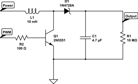
Here’s a schematic of the complete boost converter circuit:
         +-------+
 VIN ----+---+   |
         |   |   |
        --- C1  |
         |   |   |
         |  | |  |
         |  | +--+--+
         |  |    |  |
         |  +----+  |
         |          |
         |   U1   +-+
         |  555   |
         +-------+|
                 GND
                  |
                  |        D1
     L1          | +-------+---+
 +--(((((---+----|-| IRLML2502 |     C3
 |          |     +-------+---+---||----+
 |          |             |            |
 |          |             +-----+------+
 |          |                   |
 |          |                  GND
 |          |
 |          |
 +----------+
Step 7: Build and Test the Circuit
With the schematic designed, you can now build the actual circuit on a breadboard or PCB. Be sure to use proper soldering techniques and follow standard safety precautions when working with electronic circuits.
Once the circuit is built, you can test it by connecting a variable DC power supply to the input and a multimeter or oscilloscope to the output. Slowly increase the input voltage from 3.3V to 4.2V while monitoring the output voltage. You should see a steady 5V output, with some small amount of ripple.
If the output voltage is too high or too low, you may need to adjust the duty cycle by changing the values of the resistors connected to the 555 timer. If the output is unstable or the circuit gets hot, double-check your connections and component values.

Troubleshooting and Optimization
Even with careful design and construction, issues can arise when building and testing a voltage boosting circuit. Here are some common problems and how to troubleshoot them:
Output voltage is too low
- Check the input voltage to ensure it is within the expected range.
- Verify that the inductor and capacitor values are correct and that the components are not damaged.
- Check the duty cycle of the PWM signal and adjust if necessary.
Output voltage is too high
- Verify that the diode is connected with the correct polarity.
- Check the duty cycle of the PWM signal and adjust if necessary.
- Make sure the load is connected and drawing the expected current.
Output voltage is unstable or has excessive ripple
- Make sure all connections are secure and components are properly soldered.
- Increase the output capacitance to reduce ripple.
- Check for any damaged or overheated components, especially the inductor and switch.
Circuit overheats or components fail
- Verify that the switch and diode are rated for the expected current and voltage levels.
- Check for shorts or incorrect connections that could cause excessive current draw.
- Make sure the inductor is not saturating by using a larger inductor value or reducing the load current.
Once the circuit is functioning properly, you may want to optimize it for efficiency or size. Some ways to improve the performance of a voltage boosting circuit include:
- Using a synchronous rectification scheme, where a second MOSFET replaces the diode to reduce conduction losses.
- Implementing soft-switching techniques, such as zero-voltage switching (ZVS) or zero-current switching (ZCS), to reduce switching losses.
- Using a multi-phase design, where multiple boost converters operate in parallel to share the load current and reduce component stress.
- Optimizing the PCB layout to minimize trace inductance and resistance, which can improve efficiency and reduce EMI.

Conclusion
Building a voltage boosting circuit can be a fun and rewarding project for anyone interested in power electronics. By understanding the basic principles of boost converters and following a systematic design process, you can create a circuit that efficiently steps up a low voltage to a higher level.
However, it’s important to remember that working with high voltages and currents can be dangerous, so always take proper safety precautions and consult with experienced professionals if you’re unsure about any aspect of your design.
With the knowledge gained from this guide, you should be well-equipped to tackle your own voltage boosting projects and explore the fascinating world of power electronics.
Frequently Asked Questions (FAQ)
1. What is the maximum voltage a boost converter can output?
In theory, a boost converter can output an arbitrarily high voltage, limited only by the ratings of the components and the breakdown voltage of the switch and diode. In practice, the maximum output voltage is usually limited by the desired efficiency, size, and cost of the circuit. Most practical boost converters have a maximum output voltage of a few tens of volts.
2. Can a boost converter be used to charge a battery?
Yes, a boost converter can be used as part of a battery charging circuit. By regulating the output voltage and current of the boost converter, it can provide the proper charging profile for a variety of battery chemistries. However, additional circuitry may be needed to ensure safe and efficient charging, such as over-voltage and over-current protection, temperature monitoring, and charge termination.
3. How do I select the right components for my boost converter?
Choosing the right components for your boost converter depends on several factors, including the input and output voltage ranges, the expected load current, the desired efficiency, and the available space. Key components to consider are:
- Inductor: Choose an inductor with a high enough current rating and a low DC resistance to minimize losses. The inductor value should be chosen to provide the desired ripple current and avoid saturation.
- Switch: Use a MOSFET or IGBT with a low on-resistance and fast switching speeds to minimize conduction and switching losses. Make sure the switch is rated for the maximum voltage and current in the circuit.
- Diode: Select a diode with a low forward voltage drop and fast recovery time to minimize conduction losses. Schottky diodes are often used in low-voltage boost converters for their low forward voltage.
- Capacitors: Use capacitors with low ESR (equivalent series resistance) and high ripple current ratings to minimize losses and ensure reliable operation. Ceramic capacitors are a good choice for low-voltage, high-frequency applications.
4. What are some common applications for voltage boosting circuits?
Voltage boosting circuits are used in a wide range of applications, including:
- Battery-powered devices, such as smartphones, laptops, and portable electronics, where a higher voltage is needed than the battery can directly provide.
- Renewable energy systems, such as solar panels and wind turbines, where the output voltage needs to be stepped up to charge batteries or feed into the power grid.
- Automotive systems, such as headlights, fuel injectors, and audio amplifiers, which require higher voltages than the typical 12V car battery.
- Industrial control systems, where low-voltage sensors and actuators need to interface with higher-voltage control circuitry.
- LED drivers, where a constant current at a higher voltage is needed to power strings of multiple LEDs in series.
5. Can a voltage boosting circuit be used for AC voltages?
No, a basic boost converter only works with DC voltages. To step up AC voltages, you would need to use a transformer or a more complex circuit topology, such as a resonant converter or a matrix converter. These circuits are beyond the scope of this guide, but the same basic principles of energy transfer and voltage conversion apply.
I hope this article provides a comprehensive guide on how to build and troubleshoot a voltage boosting circuit. Let me know if you have any other questions!
No responses yet