Introduction to VCOs and PLLs in RF Designs
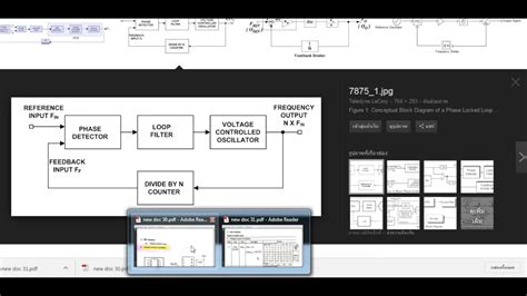
Voltage Controlled Oscillators (VCOs) and Phase Locked Loops (PLLs) are critical building blocks in many radio frequency (RF) systems implemented on printed circuit boards (PCBs). VCOs generate a adjustable frequency output signal by varying an input control voltage. PLLs use feedback to lock the phase of a VCO output to a stable reference frequency, providing a clean, programmable frequency synthesizer.
VCOs and PLLs enable frequency agility, modulation, and synchronization between transmit and receive chains in applications like:
- Wireless communications (5G, LTE, Wi-Fi, Bluetooth, etc.)
- Radar and electronic warfare
- Test and measurement equipment
- Microwave backhaul links
- Satellite transceivers
Implementing high-performance, low-noise VCOs and PLLs requires carefully optimized PCB layout techniques. Poor layout leads to unwanted coupling, spurious emissions, and degraded phase noise that can ruin RF system performance. Let’s examine best practices for VCO and PLL layout to achieve pristine synthesized local oscillator (LO) signals in your RF designs.
Key Specifications for RF VCOs and PLLs
Before diving into PCB layout, it’s important to understand the critical performance metrics that layout impacts for VCOs and PLLs:
VCO Specifications
| Spec | Description | Typical Value |
|---|---|---|
| Tuning Range | Frequency adjustment range vs control voltage | 1-10% of center freq |
| Tuning Sensitivity | Frequency change per volt (MHz/V or GHz/V) | 50-200 MHz/V |
| Phase Noise | Sideband noise power relative to carrier (dBc/Hz) | -80 to -120 dBc/Hz @ 10 kHz offset |
| Output Power | Signal power delivered to load | 0 to +10 dBm |
| Pushing | Frequency shift due to supply noise | 1-20 MHz/V |
| Pulling | Frequency shift due to load mismatch | 1-5 MHz |
| Harmonics | Power in output harmonics relative to fundamental | < -20 dBc |
PLL Specifications
| Spec | Description | Typical Value |
|---|---|---|
| Lock Range | Frequency range PLL can lock to reference | 10-100% of VCO range |
| Lock Time | Time to achieve phase lock after frequency change | 100-500 μs |
| Settling Time | Time to settle to within x Hz of final frequency | 1-10 ms |
| Phase Noise | Residual PLL phase noise (additive to VCO noise) | < -100 dBc/Hz |
| Spur Suppression | Attenuation of reference spurs | > 50 dBc |
| Noise Floor | Wideband noise power spectral density | < -150 dBm/Hz |
The PCB layout techniques covered below aim to optimize these key specs.
VCO Layout Best Practices
Proper VCO layout hinges on separating sensitive analog VCO circuitry from noisy digital synthesizer logic, carefully controlling Return current paths, and minimizing stray coupling. Follow these guidelines:
VCO Placement and Partitioning
- Place VCO core components close together in compact area
- Partition VCO on separate PCB layer from other circuitry
- Provide dedicated VCO ground plane and power planes
- Separate VCO from PLL synthesizer, avoid overlapping
- Locate VCO near board edge for shielding can
- Buffer and route VCO output away from VCO core
VCO Bypass and Decoupling
- Place VCO supply decoupling caps close to VCO
- Use large bulk decoupling cap (1-10 μF) in parallel with small RF caps (100 pF)
- Put RF chokes or ferrites in VCO bias lines to block noise
- Connect decoupling caps directly to VCO ground plane
- Avoid vias in VCO supply lines, use wide pours
VCO Signal Routing
- Route VCO tuning voltage input away from VCO output
- Avoid crossing VCO tune line over power or ground planes
- Consider microstrip for tune line over dedicated ground plane
- Terminate VCO output with resistive pi-pad for broadband match
- Route VCO output symmetrically if going to differential RFICs
- Keep VCO output away from phase detector input
VCO Shielding
- Enclose VCO circuitry in grounded shield can, solder to VCO ground plane
- Connect VCO ground to chassis at single point near VCO
- Avoid apertures or slots in VCO shielding to minimize radiation
- Use microwave absorber material inside shield can if space permits

PLL Synthesizer Layout Guidelines
The PLL synthesizer IC, typically with integrated phase-frequency detector (PFD), charge pump, and programmable dividers, is less sensitive than the VCO but still requires good layout:
PLL Placement
- Locate PLL synthesizer away from VCO core
- Group loop filter components close to PLL chip
- Place PLLVCO as close to PLL as possible
- Keep PLL away from board edges to avoid interference
- Put ground plane beneath PLL, avoid splits
PLL Power
- Use dedicated PLL analog and digital supplies
- Place analog and digital decoupling close to pins
- Put ferrites in AVDD line for PLL and VCO supply
- Connect PLL AGND and DGND together at single point
- Route power as wide pours, avoid daisy-chaining
PLL Routing
- Make reference input and feedback paths as symmetric as possible
- Keep PFD input lines short and away from I/O
- Route charge pump output directly to loop filter
- Keep loop filter components on same layer, avoid vias
- Connect loop filter output to dedicated VCO tune pin
- Route status/lock detect away from sensitive analog traces
PLL Grounding
- Connect analog and digital ground planes together near PLL
- Do not route noisy digital currents through analog ground plane
- Avoid ground loops, use star ground topology
- Connect PLL exposed paddle directly to solid ground plane
Optimizing PLL Loop Filter Design
The loop filter is critical to PLL performance, as it controls dynamics, bandwidth, and overall stability. Optimize it with these tips:
Loop Filter Topology
- Use passive 2nd or 3rd order filter for most PLLs
- Consider active 4th order for very low bandwidths (<1 kHz)
- Avoid noise gain peaking, keep ample phase margin (>45°)
- Simulate filter to verify transfer function and margins
Loop Filter Components
- Use high-Q, C0G/NP0 capacitors in filter
- Consider low-ESR tantalum for charge pump capacitor
- Place filter capacitors close to each other
- Put resistors in series with capacitors to reduce Q
- Keep filter components away from noisy digital traces
Loop Bandwidth Selection
- Choose bandwidth based on phase noise, spur, and settling time tradeoff
- Typical bandwidths 10-100 kHz for integer-N, 100-500 kHz for fractional-N
- Higher bandwidths suppress VCO noise, but amplify REFIN noise
- Lower bandwidths better reject REFIN spurs, but slow lock time
- Simulate PLL phase noise with different bandwidths to optimize
Testing and Debugging VCO/PLL Designs
Once you’ve completed your VCO and PLL PCB layout, it’s time to bring up the board and verify performance. Try these tips for efficient bringup:
VCO Bringup Steps
- Verify VCO core bias voltages and currents
- Inject DC tuning voltage, sweep to test tuning range
- Buffer VCO output and check power level and spectrum
- Measure VCO phase noise on spectrum analyzer at several offsets
- Check VCO supply pushing by modulating VLDO and observing frequency shift
- Verify minimal VCO pulling with load mismatch
PLL Bringup Procedure
- Power up PLL board with VCO tuning voltage set to midrange
- Program PLL to free-run near desired output frequency
- Monitor divided VCO output on PFD to verify signal presence
- Check lock detect status, if unlocked, reduce frequency step size
- Once locked, measure PLL phase noise, compare to simulation
- Perform transient test, e.g. frequency hop, to verify settling time
- Sweep PLL across frequency range, plot spur and noise levels
Common VCO/PLL Debug Issues
- VCO not oscillating: Check bias, reduce L or C in tank, try active bias
- VCO frequency range too narrow: Increase varactor C or decrease inductor L
- VCO phase noise too high: Increase bias current, use lower-noise devices
- PLL not locking: Check PFD inputs, loop filter values, reduce tuning step size
- PLL spur levels too high: Increase REFIN power, raise charge pump current
- PLL lock time too slow: Widen loop filter bandwidth, use fractional-N architecture
VCO and PLL PCB Layout FAQ
Q: What’s the most important factor in VCO PCB layout?
A: Isolating the VCO from sources of supply and ground noise. Use a dedicated VCO ground plane, filter bias lines, and shield the VCO thoroughly to minimize AM-to-PM noise conversion.
Q: How important is the symmetry of the PLL feedback path?
A: Very important for optimal PLL phase noise and spurs. Keep the reference and feedback lines to the phase-frequency detector well-matched in length and routing to avoid introducing unequal delays that can degrade PLL performance.
Q: What’s a good rule of thumb for PLL loop bandwidth?
A: Generally, set the loop bandwidth 1/10 to 1/20 of the reference frequency for integer-N PLLs, or 1/5 to 1/10 of REFIN for fractional-N PLLs. This provides a good balance between response time, noise suppression, and spur rejection.
Q: How do I select VCO decoupling capacitor values?
A: Use the largest value (1-10 μF) that still offers low ESR and good high-frequency performance for bulk decoupling of the VCO supply. Complement this with smaller RF capacitors (100pF – 1nF) placed very close to the VCO supply pin to filter high-frequency noise.
Q: What’s the best way to test VCO microphonics?
A: Set up the VCO with a low-noise DC supply, then inject an acoustic signal using an audio speaker placed near the VCO. Monitor the VCO output on a spectrum analyzer and look for sidebands that correlate with the audio tone. Use sound-absorbing material or mechanical isolation to mitigate microphonics.
Conclusion
Voltage controlled oscillators and phase-locked loops form the heart of frequency synthesis in modern RF systems. Achieving the highest level of performance from these critical building blocks demands thoughtful, disciplined PCB layout practices. By following the guidelines presented here – separating sensitive analog signals, minimizing unintended coupling, optimizing grounding and bypassing, and carefully tuning loop dynamics – you’ll be well on your way to creating low-noise, highly-stable frequency sources for your RF designs. Happy laying out!
No responses yet