
Introduction to EMI in High-Speed PCB Design
In today’s world of high-speed electronic devices, printed circuit boards (PCBs) play a crucial role in ensuring reliable and efficient performance. However, as signal speeds and frequencies continue to increase, electromagnetic interference (EMI) has become a significant challenge for PCB designers. EMI can cause various issues, such as signal integrity problems, crosstalk, and radiated emissions, which can degrade the overall performance of the system. To mitigate these issues, designers must employ effective techniques, such as interactive routing, to minimize the impact of EMI on high-speed PCB traces.
Understanding the Causes of EMI in PCBs
Common Sources of EMI
EMI in PCBs can originate from various sources, both internal and external to the system. Some common sources of EMI include:
- High-speed digital signals
- Switching power supplies
- Electrostatic discharge (ESD)
- Neighboring electronic devices
- Environmental factors (e.g., lightning, solar flares)
Factors Contributing to EMI Susceptibility
Several factors can make PCB traces more susceptible to EMI, including:
- Trace length and routing
- Trace impedance and termination
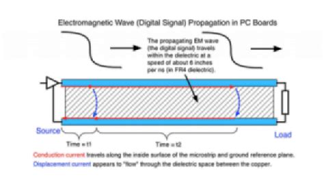
- Dielectric properties of the PCB material
- Frequency and rise/fall times of the signals
- Proximity to other traces and components
Understanding these factors is essential for designing PCBs that are more resistant to EMI.
Interactive Routing Techniques for EMI Mitigation
Interactive routing is a powerful approach to mitigating EMI issues in high-speed PCB traces. By carefully controlling the placement and routing of traces, designers can minimize the coupling between signals and reduce the overall EMI in the system.
Trace Placement and Spacing
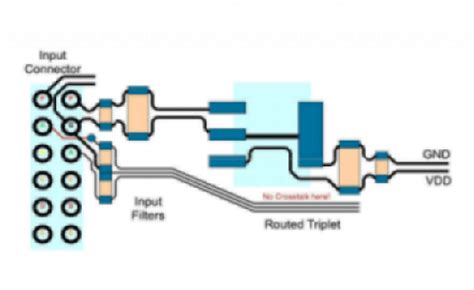
One of the most effective ways to reduce EMI is to optimize the placement and spacing of PCB traces. Some key considerations include:
- Separating sensitive traces from potential EMI sources
- Maintaining consistent spacing between parallel traces
- Avoiding long parallel runs of traces
- Using guard traces or ground planes to isolate sensitive signals
| Trace Spacing | Crosstalk Reduction |
|---|---|
| 2x trace width | 50% |
| 3x trace width | 67% |
| 4x trace width | 75% |
Impedance Control and Matching
Maintaining proper impedance control and matching is crucial for minimizing reflections and reducing EMI. Some techniques for achieving this include:
- Using controlled impedance traces (e.g., microstrip, stripline)
- Matching trace impedance to source and load impedances
- Employing termination resistors or networks
- Minimizing trace discontinuities (e.g., vias, stubs)
Differential Pair Routing
Differential signaling is a common technique used in high-speed PCB design to improve signal integrity and reduce EMI. When routing differential pairs, designers should:
- Keep the traces tightly coupled and of equal length
- Maintain a consistent spacing between the traces
- Avoid splitting the pairs or introducing discontinuities
- Use appropriate termination techniques (e.g., differential termination)
Layer Stackup and Shielding
The layer stackup and use of shielding techniques can also play a significant role in reducing EMI. Some best practices include:
- Using dedicated ground and power planes
- Placing sensitive traces on inner layers, sandwiched between ground planes
- Implementing ground stitching vias to create a low-impedance return path
- Employing shielding techniques, such as metal cans or conductive coatings

Simulation and Analysis Tools for EMI Mitigation
To effectively mitigate EMI issues in high-speed PCB designs, designers can leverage various simulation and analysis tools. These tools help identify potential problems early in the design process, allowing for more efficient and cost-effective solutions.
Pre-Layout Simulation
Pre-layout simulation tools enable designers to analyze the EMI performance of their designs before the physical layout process begins. These tools can help:
- Evaluate the impact of component placement and trace routing on EMI
- Optimize the layer stackup for better EMI performance
- Identify potential coupling and crosstalk issues
- Assess the effectiveness of shielding and grounding techniques
Post-Layout Simulation
Post-layout simulation tools allow designers to analyze the EMI performance of their designs after the physical layout is complete. These tools can:
- Perform detailed electromagnetic field simulations
- Identify potential EMI hotspots and coupling issues
- Evaluate the impact of trace geometry and spacing on EMI
- Assess the effectiveness of EMI mitigation techniques
Measurement and Testing
In addition to simulation tools, measurement and testing are essential for validating the EMI performance of high-speed PCB designs. Some common measurement techniques include:
- Near-field probing to identify EMI sources and coupling paths
- Far-field measurements to assess radiated emissions
- Time-domain reflectometry (TDR) to characterize trace impedance and discontinuities
- Spectrum analyzers to measure the frequency content of EMI signals
Best Practices for EMI Mitigation in High-Speed PCB Design
To effectively mitigate EMI issues in high-speed PCB designs, designers should follow a set of best practices that encompass various aspects of the design process.
Design Planning and Partitioning
- Identify and categorize signals based on their speed, sensitivity, and potential for EMI
- Partition the design into functional blocks, separating sensitive circuits from potential EMI sources
- Define a clear grounding and power distribution strategy
Component Selection and Placement
- Choose components with low EMI characteristics (e.g., slew rate control, spread-spectrum clocking)
- Place components to minimize the length of high-speed traces and reduce coupling
- Use shielding techniques, such as metal cans or conductive gaskets, for sensitive components
Routing and Layering
- Route high-speed traces on controlled impedance layers, such as microstrip or stripline
- Minimize the length and number of vias in high-speed traces
- Use appropriate spacing and shielding techniques to reduce crosstalk and coupling
- Implement a well-defined layer stackup with dedicated ground and power planes
Grounding and Shielding
- Create a low-impedance ground plane to provide a stable reference for high-speed signals
- Use ground stitching vias to create a continuous ground path and reduce ground bounce
- Implement shielding techniques, such as ground guard traces or conductive coatings, to reduce EMI
Simulation, Testing, and Validation
- Perform pre-layout and post-layout simulations to identify and mitigate potential EMI issues
- Conduct thorough testing and measurement to validate the EMI performance of the design
- Iterate the design process based on simulation and test results to optimize EMI mitigation
By following these best practices and employing interactive routing techniques, PCB designers can effectively mitigate EMI issues in high-speed traces and ensure the reliable and efficient performance of their electronic systems.
Frequently Asked Questions (FAQ)
-
What is EMI, and why is it a concern in high-speed PCB design?
EMI, or electromagnetic interference, refers to the unwanted coupling of electromagnetic energy between electronic components or systems. In high-speed PCB design, EMI can cause signal integrity issues, crosstalk, and radiated emissions, which can degrade the performance and reliability of the system. -
How does interactive routing help mitigate EMI issues in high-speed PCB traces?
Interactive routing is a technique that allows designers to manually control the placement and routing of PCB traces. By carefully positioning traces, maintaining consistent spacing, and using shielding techniques, designers can minimize the coupling between signals and reduce the overall EMI in the system. -
What are some common techniques for maintaining proper impedance control in high-speed PCB traces?
Some common techniques for maintaining proper impedance control include using controlled impedance traces (such as microstrip or stripline), matching trace impedance to source and load impedances, employing termination resistors or networks, and minimizing trace discontinuities (such as vias or stubs). -
How can simulation and analysis tools assist in mitigating EMI issues in high-speed PCB designs?
Simulation and analysis tools enable designers to evaluate the EMI performance of their designs before and after the physical layout process. Pre-layout simulations help optimize component placement, trace routing, and layer stackup for better EMI performance. Post-layout simulations allow for detailed electromagnetic field analysis and identification of potential EMI hotspots and coupling issues. -
What are some best practices for grounding and shielding in high-speed PCB designs to reduce EMI?
Some best practices for grounding and shielding include creating a low-impedance ground plane to provide a stable reference for high-speed signals, using ground stitching vias to create a continuous ground path and reduce ground bounce, and implementing shielding techniques (such as ground guard traces or conductive coatings) to reduce EMI. Additionally, a well-defined layer stackup with dedicated ground and power planes can help minimize EMI issues.
No responses yet