Introduction to USB-ULPI Routing
USB (Universal Serial Bus) has become the standard interface for connecting peripherals to computers and mobile devices. With the increasing demand for faster data transfer speeds, the USB 3.0 standard was introduced, offering theoretical speeds up to 5 Gbps. To achieve these high speeds, proper routing of the USB signals is crucial, especially when using the ULPI (UTMI+ Low Pin Interface) protocol. In this article, we will dive into the details of USB-ULPI routing, discussing best practices, challenges, and solutions.
What is ULPI?
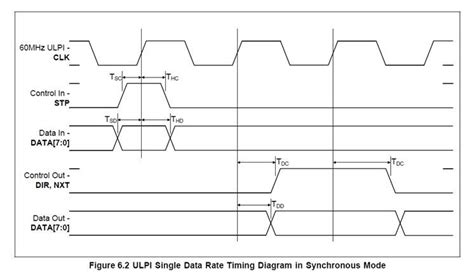
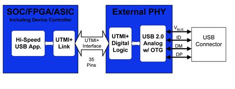
ULPI is a standard interface protocol for connecting USB 3.0 PHY (Physical Layer) to USB 3.0 controllers. It is designed to reduce the number of pins required for the interface, making it more suitable for mobile and embedded devices. ULPI uses a 12-pin interface, which includes 8 data lines, a clock line, a direction line, and power and ground pins.
Importance of Proper USB-ULPI Routing
Proper routing of USB-ULPI signals is essential to ensure reliable and efficient data transfer. Poor routing can lead to signal integrity issues, resulting in data corruption, intermittent connections, and even device failures. Additionally, improper routing can cause electromagnetic interference (EMI), which can affect nearby components and cause compliance issues.
USB-ULPI Routing Guidelines
To ensure optimal USB-ULPI routing, follow these guidelines:
1. Maintain Controlled Impedance
USB-ULPI signals require a controlled impedance of 50 ohms to minimize reflections and maintain signal integrity. This can be achieved by using appropriate PCB (Printed Circuit Board) stackup and trace geometries. The trace width and spacing should be calculated based on the PCB material’s dielectric constant and thickness.
2. Keep Traces Short and Direct
To minimize signal attenuation and distortion, keep USB-ULPI traces as short and direct as possible. Avoid unnecessary turns and vias, as they can introduce impedance discontinuities and increase signal reflections. If vias are unavoidable, use micro vias to minimize their impact on signal integrity.
3. Maintain Proper Trace Spacing
Maintain adequate spacing between USB-ULPI traces to minimize crosstalk and interference. The spacing should be calculated based on the trace geometry, signal speed, and PCB material properties. As a general rule, keep a minimum spacing of 3 times the trace width between adjacent traces.
4. Use Differential Pair Routing
USB-ULPI data lines (D0-D7) are differential pairs and should be routed as such. Differential pair routing helps to cancel out common-mode noise and maintain signal integrity. Ensure that the differential pairs have matched lengths and are routed closely together to minimize any phase difference between the signals.
5. Implement Ground Shielding
To reduce EMI and crosstalk, implement ground shielding around the USB-ULPI traces. This can be done by placing ground planes above and below the signal layer, as well as using guard traces or coplanar waveguides. Ground shielding helps to contain the electromagnetic fields generated by the high-speed signals and prevents them from interfering with other components.
6. Decouple Power Lines
Proper decoupling of the USB-ULPI power lines is crucial to ensure stable operation and minimize noise. Place decoupling capacitors as close as possible to the PHY and controller power pins. Use a combination of bulk and ceramic capacitors to provide low and high-frequency decoupling. The capacitor values and placement should be determined based on the specific design requirements and the manufacturer’s recommendations.
USB-ULPI Routing Challenges and Solutions
Routing USB-ULPI signals can present several challenges, especially in dense and complex PCB designs. Some common challenges and their solutions include:
1. Limited PCB Space
In space-constrained designs, it can be challenging to route USB-ULPI traces while maintaining proper spacing and shielding. To overcome this, consider using higher layer count PCBs or advanced PCB manufacturing techniques such as HDI (High-Density Interconnect) or blind and buried vias. These techniques allow for more efficient use of PCB space and can help to minimize the impact of high-speed signals on other components.
2. Signal Integrity Issues
Signal integrity issues, such as reflections, crosstalk, and EMI, can be more pronounced in USB-ULPI routing due to the high signal speeds involved. To mitigate these issues, use simulation tools to analyze the signal behavior and optimize the PCB layout accordingly. Additionally, consider using signal conditioning techniques, such as pre-emphasis and equalization, to compensate for signal losses and distortions.
3. Manufacturing Constraints
USB-ULPI routing may require advanced PCB manufacturing capabilities, such as tight tolerances, controlled impedance, and high-speed materials. It is essential to work closely with the PCB manufacturer to ensure that the design can be manufactured reliably and cost-effectively. Provide clear and comprehensive documentation, including stackup, impedance, and spacing requirements, to avoid any misunderstandings or delays in the manufacturing process.

USB-ULPI Routing Best Practices
To summarize, here are some best practices for USB-ULPI routing:
- Use a PCB stackup with controlled impedance and appropriate dielectric materials.
- Keep USB-ULPI traces as short and direct as possible, minimizing turns and vias.
- Maintain proper trace spacing to minimize crosstalk and interference.
- Route USB-ULPI data lines as differential pairs with matched lengths.
- Implement ground shielding around USB-ULPI traces to reduce EMI.
- Decouple USB-ULPI power lines using a combination of bulk and ceramic capacitors.
- Use simulation tools to analyze signal integrity and optimize the PCB layout.
- Work closely with the PCB manufacturer to ensure reliable and cost-effective manufacturing.
By following these guidelines and best practices, designers can ensure robust and reliable USB-ULPI routing, enabling high-speed data transfer in their designs.
USB-ULPI Routing Examples
To better understand USB-ULPI routing, let’s look at some practical examples.
Example 1: Simple USB-ULPI Routing
In this example, we have a basic USB-ULPI interface between a USB 3.0 controller and a USB 3.0 PHY. The PCB stackup consists of four layers: top signal, ground, power, and bottom signal. The USB-ULPI traces are routed on the top layer, with ground shielding on the layer below.
| Layer | Description |
|---|---|
| Top | Signal (USB-ULPI traces) |
| Layer 2 | Ground |
| Layer 3 | Power |
| Bottom | Signal |
The USB-ULPI traces are routed as follows:
- Data lines (D0-D7) are routed as differential pairs with a trace width of 0.15 mm and a spacing of 0.15 mm between the pairs.
- The clock line (CLK) is routed with a trace width of 0.15 mm.
- The direction line (DIR) is routed with a trace width of 0.15 mm.
- Power (VCC) and ground (GND) are routed with a trace width of 0.3 mm.
Decoupling capacitors (0.1 µF and 10 µF) are placed close to the PHY and controller power pins.
Example 2: High-Density USB-ULPI Routing
In this example, we have a more complex design with multiple USB-ULPI interfaces and limited PCB space. The PCB stackup consists of six layers: top signal, ground, inner signal 1, inner signal 2, power, and bottom signal. The USB-ULPI traces are routed on the inner signal layers, with ground shielding on the adjacent layers.
| Layer | Description |
|---|---|
| Top | Signal |
| Layer 2 | Ground |
| Layer 3 | Signal (USB-ULPI traces) |
| Layer 4 | Signal (USB-ULPI traces) |
| Layer 5 | Power |
| Bottom | Signal |
To accommodate the high-density routing, the following techniques are used:
- Data lines (D0-D7) are routed as differential pairs with a trace width of 0.1 mm and a spacing of 0.1 mm between the pairs.
- The clock line (CLK) and direction line (DIR) are routed with a trace width of 0.1 mm.
- Power (VCC) and ground (GND) are routed with a trace width of 0.2 mm.
- Blind and buried vias are used to transition between layers, minimizing the impact on signal integrity.
- Coplanar waveguides are used to provide additional ground shielding around the USB-ULPI traces.
Decoupling capacitors (0.1 µF and 10 µF) are placed close to the PHY and controller power pins, and additional decoupling capacitors (0.01 µF) are placed along the power traces to provide local decoupling.
By carefully planning the PCB stackup, using advanced routing techniques, and implementing proper shielding and decoupling, even high-density USB-ULPI designs can be successfully routed while maintaining signal integrity.
Frequently Asked Questions (FAQ)
-
What is the difference between USB 2.0 and USB 3.0 routing?
USB 3.0 operates at much higher speeds compared to USB 2.0, requiring more stringent routing guidelines. USB 3.0 uses differential signaling and requires controlled impedance routing, while USB 2.0 uses single-ended signaling and is more forgiving in terms of routing. -
Can I route USB-ULPI traces on the same layer as other signals?
It is generally recommended to route USB-ULPI traces on dedicated signal layers to minimize interference and crosstalk. If routing on the same layer as other signals is unavoidable, ensure proper spacing and shielding to minimize any potential issues. -
How do I calculate the required trace width and spacing for USB-ULPI routing?
The trace width and spacing for USB-ULPI routing depend on several factors, including the PCB material properties, stackup, and target impedance. Use a PCB calculator or simulation tool to determine the appropriate values based on your specific design requirements. -
What are the consequences of improper USB-ULPI routing?
Improper USB-ULPI routing can lead to signal integrity issues, such as reflections, crosstalk, and EMI. These issues can cause data corruption, intermittent connections, device failures, and non-compliance with USB standards. -
Can I use autorouting for USB-ULPI traces?
While autorouting can be used for USB-ULPI traces, it is recommended to manually route the critical signals to ensure proper spacing, shielding, and impedance control. Autorouting algorithms may not always consider the specific requirements of high-speed signals, leading to suboptimal results.
Conclusion
USB-ULPI routing is a critical aspect of designing high-speed USB 3.0 interfaces. Proper routing techniques, including controlled impedance, differential pair routing, ground shielding, and decoupling, are essential to maintain signal integrity and ensure reliable data transfer. By understanding the challenges and best practices associated with USB-ULPI routing, designers can create robust and efficient designs that meet the growing demands for high-speed connectivity in modern electronic devices.
No responses yet