What is a PCB Netlist?
A PCB (Printed Circuit Board) netlist is a comprehensive list that contains information about the electronic components and their interconnections on a PCB. It serves as a crucial link between the schematic design and the physical layout of the PCB. The netlist is a text file that follows a specific format, such as ASCII or XML, and is generated by Electronic Design Automation (EDA) tools after the schematic capture process.
The primary purpose of a PCB netlist is to provide a complete description of the circuit, including:
- Component information (e.g., part numbers, values, and footprints)
- Net information (e.g., net names, connected pins, and net classes)
- Design constraints (e.g., component placement, routing rules, and electrical requirements)
Types of PCB Netlists
There are several types of PCB netlists, each serving a specific purpose in the PCB design process:
| Netlist Type | Description |
|---|---|
| Schematic Netlist | Generated from the schematic design, containing component and net information |
| PCB Netlist | Generated from the PCB layout, including physical information like component placement and routing |
| Bill of Materials (BOM) | A list of all components used in the design, with their quantities, part numbers, and other relevant information |
| SPICE Netlist | Used for circuit simulation and analysis, containing component models and their interconnections |
Why is a PCB Netlist Important?
A PCB netlist is essential for several reasons:
-
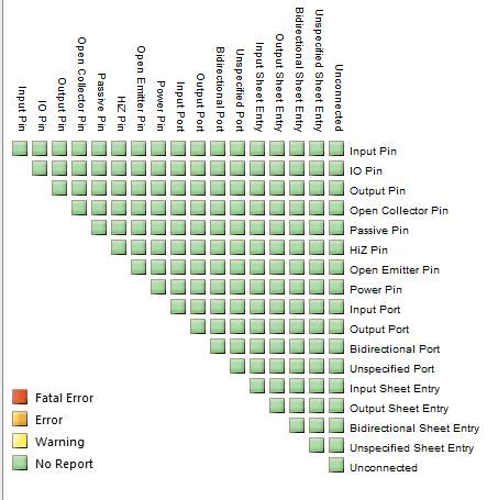
Design Verification: The netlist allows for design rule checks (DRC) and electrical rule checks (ERC) to ensure the design meets the specified constraints and requirements.
-
PCB Layout: The netlist is imported into the PCB layout software to guide the placement and routing of components, ensuring the physical design matches the schematic.
-
Manufacturing: The netlist is used to generate the necessary files for PCB fabrication, such as Gerber files, drill files, and pick-and-place files.
-
Collaboration: Netlists facilitate collaboration between team members, as they can be shared and used to transfer design information between different EDA tools and design stages.
Common Netlist Formats
There are several common netlist formats used in the PCB design industry:
| Format | Description |
|---|---|
| EDIF | Electronic Design Interchange Format, a neutral format for exchanging design data between different EDA tools |
| PADS | A proprietary format used by the PADS PCB design software |
| OrCAD | A proprietary format used by the OrCAD PCB design software |
| Protel | A proprietary format used by the Altium Designer PCB design software |
| KiCad | An open-source format used by the KiCad PCB design software |
How to Generate a PCB Netlist
Generating a PCB netlist typically involves the following steps:
-
Schematic Capture: Create the schematic design using an EDA tool, placing components and defining their interconnections.
-
Design Rule Setup: Define the design rules and constraints, such as net classes, component placement requirements, and routing rules.
-
Annotation: Assign unique identifiers to the components in the schematic, ensuring consistency between the schematic and the netlist.
-
Netlist Generation: Use the EDA tool’s built-in functionality to generate the netlist file, selecting the appropriate format and options.
-
Error Checking: Review the generated netlist for any errors or warnings, and address them before proceeding to the PCB layout stage.
Tips for Creating a High-Quality PCB Netlist
To ensure a smooth PCB design process and minimize issues, consider the following tips when creating a PCB netlist:
-
Use consistent naming conventions: Adopt a clear and consistent naming scheme for components, nets, and other design elements to avoid confusion and errors.
-
Define net classes: Group nets with similar requirements (e.g., power, ground, signal) into net classes, making it easier to apply design rules and constraints.
-
Validate the schematic: Perform thorough error checking and design rule validation on the schematic before generating the netlist.
-
Use appropriate component footprints: Ensure that the selected component footprints match the actual components to be used in the design, preventing issues during PCB layout and manufacturing.
-
Document design decisions: Maintain clear documentation of design decisions, constraints, and requirements to facilitate collaboration and future revisions.

Interpreting a PCB Netlist
Understanding how to read and interpret a PCB netlist is crucial for designers, as it allows them to verify the design and troubleshoot any issues. A typical netlist contains the following sections:
-
Header: Provides general information about the netlist, such as the file format, creation date, and EDA tool used.
-
Component List: Lists all the components in the design, with their reference designators, part numbers, and footprints.
-
Net List: Defines the interconnections between components, listing the net names and the pins connected to each net.
-
Design Rules: Specifies the design constraints and requirements, such as net classes, component placement rules, and routing rules.
Here’s an example of a simple PCB netlist in ASCII format:
(export (version D)
  (design
    (source "C:\example\schematic.sch")
    (date "2023-04-20 10:30:00")
    (tool "EDA Tool")
  )
  (components
    (comp (ref R1)
      (value 1k)
      (footprint Resistor_SMD:R_0805_2012Metric)
    )
    (comp (ref C1)
      (value 10uF)
      (footprint Capacitor_SMD:C_0805_2012Metric)
    )
    (comp (ref U1)
      (value LM358)
      (footprint Package_SO:SOIC-8_3.9x4.9mm_P1.27mm)
    )
  )
  (nets
    (net (code 1) (name "VCC")
      (node (ref R1) (pin 1))
      (node (ref U1) (pin 8))
    )
    (net (code 2) (name "GND")
      (node (ref C1) (pin 2))
      (node (ref U1) (pin 4))
    )
    (net (code 3) (name "IN")
      (node (ref R1) (pin 2))
      (node (ref U1) (pin 3))
    )
    (net (code 4) (name "OUT")
      (node (ref C1) (pin 1))
      (node (ref U1) (pin 1))
    )
  )
)
In this example, the netlist defines three components (R1, C1, and U1) and four nets (VCC, GND, IN, and OUT). Each component is listed with its reference designator, value, and footprint, while each net is defined by its name and the pins connected to it.
PCB Netlist Best Practices
To optimize your PCB design process and ensure the best possible results, consider adopting the following best practices when working with PCB netlists:
-
Use a version control system: Manage your design files, including netlists, using a version control system like Git to track changes and facilitate collaboration.
-
Perform regular design reviews: Conduct periodic design reviews to catch errors early and ensure the design meets the specified requirements.
-
Use automated testing: Implement automated testing procedures to validate the netlist and catch any issues before proceeding to PCB layout.
-
Maintain a component library: Create and maintain a centralized component library with up-to-date information on component footprints, 3D models, and other relevant data.
-
Collaborate with manufacturers: Work closely with PCB manufacturers to ensure your netlist and design files are compatible with their processes and requirements.
Frequently Asked Questions (FAQ)
-
What is the difference between a schematic netlist and a PCB netlist?
A schematic netlist contains information about the components and their interconnections based on the schematic design, while a PCB netlist also includes physical information like component placement and routing from the PCB layout. -
Can I use different EDA tools for schematic capture and PCB layout?
Yes, you can use different EDA tools for schematic capture and PCB layout, as long as they support a common netlist format like EDIF for exchanging design data. -
How do I troubleshoot errors in my PCB netlist?
To troubleshoot errors in your PCB netlist, first review the error messages provided by the EDA tool. Common issues include missing or incorrect component information, unconnected nets, and design rule violations. Double-check your schematic and design rules, and consult the EDA tool’s documentation for guidance on resolving specific errors. -
What should I do if my PCB netlist is incompatible with my manufacturer’s requirements?
If your PCB netlist is incompatible with your manufacturer’s requirements, contact them for guidance on the necessary adjustments. This may involve updating your component library, modifying design rules, or generating the netlist in a different format. -
How often should I generate a new PCB netlist during the design process?
It’s a good practice to generate a new PCB netlist whenever significant changes are made to the schematic or design rules. This ensures that the PCB layout always reflects the most up-to-date design information. Additionally, generate a final netlist before sending the design files for manufacturing.
Conclusion
A PCB netlist is a critical component of the PCB design process, serving as the bridge between schematic capture and PCB layout. By understanding the structure, importance, and best practices associated with PCB netlists, designers can create more efficient, accurate, and manufacturable designs. Regular design reviews, automated testing, and collaboration with manufacturers are key to ensuring the success of your PCB projects.
As you work with PCB netlists, remember to maintain clear documentation, use consistent naming conventions, and stay updated with industry standards and best practices. By mastering the art of PCB netlist management, you’ll be well-equipped to tackle even the most complex PCB designs with confidence.
No responses yet