Breadboard vs Prototype: Key Differences to Consider
When developing electronic circuits and projects, hobbyists and engineers often start by creating a prototype on a breadboard for quick testing and iteration. However, there are important differences between breadboard prototypes and fully developed printed circuit board (PCB) prototype layouts that impact the design process. In this article, we’ll explore the key nuances between breadboarding and prototyping to help you transition your project from concept to manufacturable product.
Breadboards: Great for Quick Proofs-of-Concept
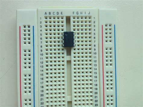
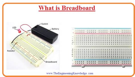
Breadboards are an essential tool for rapidly assembling temporary electronic circuits without any soldering. They consist of a perforated block of plastic with many tin-plated phosphor bronze or nickel silver alloy spring clips underneath. These clips are designed to hold wires and the leads of electronic components, allowing you to easily insert and remove parts to modify your circuit as needed.
Advantages of breadboards include:
- Quick and easy to use
- No soldering required
- Parts can be reused
- Convenient for testing circuit modifications
- Low cost
However, breadboards also have some limitations:
- Less durable than PCBs
- Not suitable for high frequency circuits due to parasitic capacitance
- Prone to loose connections and mechanical instability
- Large footprint compared to PCBs
- Not designed for permanent installations
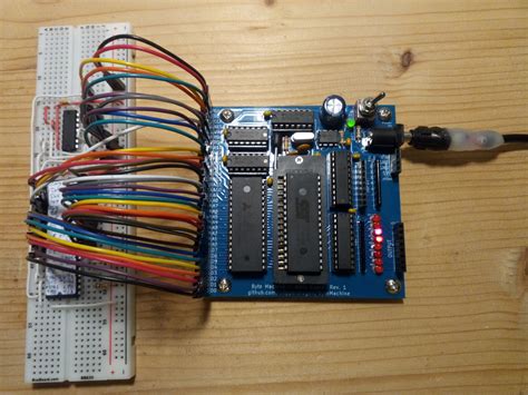
Despite these drawbacks, breadboards remain an indispensable prototyping tool, especially in the early concept phases of a project. They allow you to quickly test ideas and iterate on your design without investing time and resources into fabricating a custom PCB.
Prototype Layouts: The Next Step Toward Production
Once you have a working breadboard prototype, the next step is usually to transition your design to a custom PCB. This involves creating a schematic diagram that represents the electrical connections of your circuit, followed by a PCB layout that physically arranges the components and routes the traces between them.
PCB prototype layouts offer several advantages over breadboards:
- Compact size and lower profile
- Improved mechanical stability and durability
- Reduced electromagnetic interference (EMI) and parasitic effects
- Easier to replicate and scale up production
- Professional appearance
However, creating a PCB prototype also requires additional skills and tools compared to breadboarding:
- Proficiency with electronic design automation (EDA) software
- Knowledge of PCB design rules and best practices
- Access to PCB fabrication and assembly services
- Higher upfront costs for small quantities
Despite these challenges, transitioning to a PCB prototype is a crucial step in developing a production-ready electronic product. It allows you to validate your design in a form factor that closely resembles the final product, and it provides a foundation for further optimization and refinement.
Transitioning from Breadboard to Prototype: Best Practices
To smoothly transition your project from a breadboard to a PCB prototype, consider the following best practices:
1. Create a Detailed Schematic
Before laying out your PCB, create a comprehensive schematic diagram that captures all the electrical connections in your circuit. Use hierarchical design techniques to break down complex circuits into smaller, more manageable sections. Assign unique reference designators to each component, and use consistent naming conventions for nets and signals.
2. Choose the Right PCB Form Factor
Consider the mechanical requirements of your project when selecting a PCB form factor. Common options include:
- Single-sided boards
- Double-sided boards
- Multilayer boards
- Rigid-flex boards
Factor in the available space, required component placement, and any enclosure constraints when making your decision.
3. Adhere to PCB Layout Best Practices
When laying out your PCB, follow industry-standard best practices to ensure optimal performance and manufacturability:
- Minimize trace lengths and loops to reduce EMI
- Provide adequate clearance between components and traces
- Use ground planes to improve signal integrity
- Route power traces wider than signal traces
- Avoid acute angles in traces to prevent acid traps during etching
- Add solder mask and silkscreen layers for easier assembly and debugging
Consult with your PCB fabrication and assembly partners to ensure your design meets their specific requirements and guidelines.
4. Prototype Early and Often
Develop a prototype as soon as possible to identify any issues or areas for improvement in your design. Start with a basic proof-of-concept prototype to validate key functionality, then iterate and refine your design based on testing and user feedback. Consider using rapid prototyping techniques like 3D printing to create enclosures and mechanical parts in parallel with PCB development.
5. Plan for Manufacturing
As you finalize your PCB prototype, start planning for the manufacturing phase. Research and select reliable PCB fabrication and assembly partners, and communicate your requirements clearly. Consider factors like lead times, minimum order quantities, and pricing to ensure your project stays on schedule and within budget.
Common Pitfalls to Avoid
When transitioning from a breadboard to a PCB prototype, watch out for these common pitfalls:
1. Overlooking Power Requirements
Breadboard prototypes often use bench power supplies or batteries, which may not be practical for the final product. When designing your PCB, consider the power requirements of your circuit and select appropriate voltage regulators, power management ICs, and connectors. Ensure your PCB can handle the expected current draw without excessive voltage drop or thermal issues.
2. Neglecting Signal Integrity
Breadboards introduce parasitic capacitance and inductance that can degrade signal integrity, especially at high frequencies. When laying out your PCB, pay close attention to signal routing and termination to minimize reflections, crosstalk, and EMI. Use simulation tools to analyze critical signals and make adjustments as needed.
3. Forgetting About Mechanical Constraints
PCBs must integrate with mechanical components like enclosures, connectors, and mounting hardware. When designing your PCB, consider the mechanical constraints of your project and leave adequate space for assembly and serviceability. Collaborate closely with mechanical engineers to ensure proper fit and function.
4. Skipping Design Reviews
Before sending your PCB out for fabrication, conduct thorough design reviews to catch any errors or oversights. Use EDA tools to run design rule checks (DRCs) and electrical rule checks (ERCs), and have a colleague review your schematic and layout. Catching mistakes early can save significant time and cost in the long run.

FAQ
1. Can I use a breadboard for my final product?
While breadboards are great for prototyping, they are not suitable for final products due to their limited durability, large size, and susceptibility to noise and interference. It’s best to transition to a custom PCB for production.
2. How much does it cost to fabricate a custom PCB?
The cost of PCB fabrication varies depending on factors like board size, layer count, quantity, and turnaround time. For small quantities (less than 100), expect to pay around $10-$50 per board, while larger volumes can reduce the unit cost significantly.
3. What software do I need to design a PCB?
To design a PCB, you’ll need electronic design automation (EDA) software that includes schematic capture and PCB layout tools. Popular options include Autodesk Eagle, KiCad, and Altium Designer, among others. Some tools offer free versions with limited features, while others require a paid license.
4. How long does it take to get a PCB prototype?
The turnaround time for PCB prototypes depends on the complexity of your design and the capabilities of your fabrication partner. Typical lead times range from a few days to a few weeks, although expedited services may be available for a higher cost.
5. What are some common PCB assembly methods?
The two main PCB assembly methods are through-hole (THT) and surface-mount (SMT). THT involves inserting component leads through holes in the board and soldering them in place, while SMT places components directly on the surface of the board using solder paste and reflow ovens. SMT is generally faster and more automated than THT, but some components may only be available in through-hole packages.
Conclusion
Transitioning from a breadboard prototype to a custom PCB is a significant milestone in the development of any electronic project. By understanding the nuances between these two approaches and following best practices for schematic design, PCB layout, and manufacturing planning, you can successfully navigate this transition and bring your ideas to life. Remember to prototype early and often, seek feedback from peers and experts, and stay flexible as you refine your design. With persistence and attention to detail, you can transform your breadboard concept into a professional-grade electronic product.
No responses yet