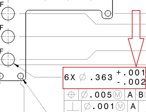
What are PCB Tolerances?
PCB (Printed Circuit Board) tolerances refer to the acceptable variations in the dimensions and properties of a PCB during the manufacturing process. These tolerances are essential to ensure that the PCB functions as intended and meets the required specifications. Two critical aspects of PCB tolerances are track width and isolation gap tolerances.
Track Width Tolerances
Track width refers to the width of the conductive paths (copper traces) on a PCB. The track width tolerance specifies the acceptable variation in the width of these traces. Factors that influence track width tolerances include:
- Manufacturing process (etching, plating, etc.)
- PCB material properties
- Copper thickness
- Required current carrying capacity
Typical track width tolerances for various copper thicknesses are shown in the table below:
| Copper Thickness (oz) | Minimum Track Width (mm) | Tolerance (mm) |
|---|---|---|
| 0.5 | 0.15 | ± 0.05 |
| 1 | 0.20 | ± 0.05 |
| 2 | 0.30 | ± 0.05 |
| 3 | 0.40 | ± 0.05 |
Isolation Gap Tolerances
Isolation gaps, also known as clearances, refer to the spacing between adjacent conductive elements on a PCB. The isolation gap tolerance specifies the acceptable variation in these spacings. Factors that influence isolation gap tolerances include:
- PCB material properties
- Voltage requirements
- Manufacturing process
Typical isolation gap tolerances for various PCB classes are shown in the table below:
| PCB Class | Minimum Isolation Gap (mm) | Tolerance (mm) |
|---|---|---|
| Class 1 | 0.20 | ± 0.05 |
| Class 2 | 0.15 | ± 0.05 |
| Class 3 | 0.10 | ± 0.05 |
Importance of PCB Tolerances
Maintaining PCB tolerances is crucial for several reasons:
-
Functionality: Proper track widths and isolation gaps ensure that the PCB functions as intended, without short circuits or signal integrity issues.
-
Reliability: Adhering to tolerances helps improve the reliability and longevity of the PCB by reducing the risk of failures due to manufacturing defects.
-
Manufacturability: Well-defined tolerances facilitate efficient and consistent PCB manufacturing, minimizing production delays and costs.
-
Compliance: Meeting industry standards and regulations for PCB tolerances is essential for ensuring product safety and compatibility.
Designing for PCB Tolerances
When designing a PCB, it is essential to consider track width and isolation gap tolerances to ensure successful manufacturing and performance. Some best practices for designing with tolerances in mind include:
-
Follow design guidelines: Adhere to the recommended track width and isolation gap values provided by the PCB manufacturer or industry standards.
-
Consider the manufacturing process: Understand the capabilities and limitations of the chosen manufacturing process and adjust the design accordingly.
-
Use appropriate design tools: Employ PCB design software that supports design rule checks (DRC) to ensure that the design meets the specified tolerances.
-
Communicate with the manufacturer: Collaborate with the PCB manufacturer to discuss tolerance requirements and any specific design considerations.

Testing and Inspection
To ensure that manufactured PCBs meet the specified tolerances, various testing and inspection methods are employed:
-
Visual inspection: Manual or automated visual inspection of the PCB to check for any visible defects or deviations from the design.
-
Automated optical inspection (AOI): Using computer vision and image processing techniques to detect and measure track widths, isolation gaps, and other features.
-
Electrical testing: Performing continuity, insulation resistance, and other electrical tests to verify the integrity of the PCB and its components.
-
Cross-sectional analysis: Cutting and examining cross-sections of the PCB to measure layer thicknesses, copper distribution, and other internal features.
Frequently Asked Questions (FAQ)
-
What happens if the track width is too narrow?
A: If the track width is too narrow, it may not be able to carry the required current, leading to overheating and potential failure of the PCB. Additionally, narrow tracks are more susceptible to manufacturing defects and may not meet the specified tolerances. -
Can I use smaller isolation gaps to save space on my PCB?
A: While using smaller isolation gaps can help save space on a PCB, it is essential to ensure that the gaps still meet the minimum requirements for the given PCB class and voltage requirements. Smaller gaps may increase the risk of short circuits and signal integrity issues. -
How can I ensure that my PCB design meets the specified tolerances?
A: To ensure that your PCB design meets the specified tolerances, follow the design guidelines provided by the manufacturer or industry standards, use appropriate design tools with DRC capabilities, and communicate with the PCB manufacturer to discuss any specific requirements or concerns. -
What are the consequences of not meeting PCB tolerances?
A: Not meeting PCB tolerances can lead to various issues, such as functional failures, reduced reliability, increased manufacturing costs, and non-compliance with industry standards or regulations. It is crucial to adhere to the specified tolerances to ensure the proper functioning and longevity of the PCB. -
Can PCB tolerances be modified after manufacturing?
A: In most cases, PCB tolerances cannot be modified after manufacturing, as they are determined by the design and manufacturing process. If tolerances are not met, the PCB may need to be redesigned or re-manufactured, which can be costly and time-consuming. Therefore, it is essential to consider tolerances during the design phase and ensure that they are achievable through the selected manufacturing process.
Conclusion
Understanding and adhering to manufacturing tolerances, particularly track width and isolation gap tolerances, is crucial for designing and producing reliable, high-quality PCBs. By considering these tolerances throughout the design process, collaborating with PCB manufacturers, and employing appropriate testing and inspection methods, designers and engineers can ensure that their PCBs meet the required specifications and perform as intended. As PCB technology continues to advance, staying informed about the latest tolerance standards and best practices will be essential for success in the electronics industry.

No responses yet