What is a Ground Plane in PCB Design?
A ground plane is a large area of copper on a printed circuit board (PCB) that is connected to the ground or 0V reference point of the circuit. In a two layer PCB, the ground plane is typically located on the bottom layer, while the top layer is used for routing signals and placing components. The ground plane serves several important functions in PCB design, including:
- Providing a low-impedance return path for current
- Reducing electromagnetic interference (EMI) and crosstalk between signals
- Improving signal integrity and reducing noise
- Helping to distribute heat evenly across the PCB
The Importance of a Proper Ground Plane
Having a properly designed ground plane is crucial for the performance and reliability of your two layer PCB. Without a good ground plane, your circuit may suffer from various issues, such as:
- Excessive noise and interference
- Poor signal quality and integrity
- Increased risk of electromagnetic compatibility (EMC) problems
- Difficulty in achieving desired impedance for high-speed signals
- Uneven heat distribution and potential thermal issues
By incorporating a well-designed ground plane into your two layer PCB, you can mitigate these issues and ensure that your circuit functions as intended.
Designing Your Ground Plane
When designing the ground plane for your two layer PCB, there are several key factors to consider, such as:
Size and Shape
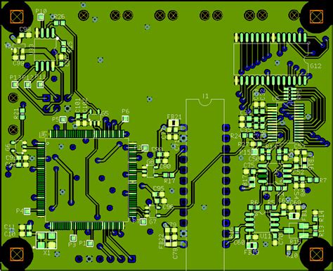
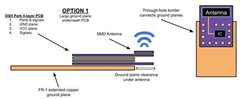
The size and shape of your ground plane will depend on the overall dimensions of your PCB and the placement of components. Ideally, the ground plane should cover as much of the PCB surface as possible, while leaving enough space for signal traces and components. In some cases, you may need to create cutouts or voids in the ground plane to accommodate specific components or to reduce the capacitance between the ground plane and certain signals.
Connectivity
It’s important to ensure that your ground plane is properly connected to all the ground points in your circuit. This can be achieved through the use of vias, which are small holes drilled through the PCB that allow signals to pass between layers. When placing vias, it’s important to consider their size, spacing, and location to minimize inductance and ensure good electrical contact.
Clearance and Spacing
When routing signals on the top layer of your two layer PCB, it’s important to maintain appropriate clearance and spacing between the signal traces and the ground plane. This helps to reduce the risk of short circuits and ensures that the desired impedance is achieved for high-speed signals. The specific clearance and spacing requirements will depend on factors such as the signal frequency, the dielectric material of the PCB, and the manufacturing capabilities of your PCB fabricator.
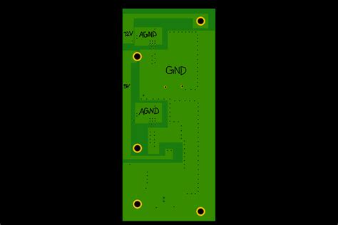
Split Planes and Power Islands
In some cases, it may be necessary to split the ground plane into separate sections or create power islands for specific components. This can help to isolate sensitive circuits from noisy ones, or to provide a separate return path for high-current signals. When splitting planes or creating power islands, it’s important to consider the current flow and ensure that there is a low-impedance connection between the different sections of the ground plane.
Common Ground Plane Issues and How to Avoid Them
Despite the benefits of having a good ground plane, there are several common issues that can arise if the ground plane is not designed properly. Some of these issues include:
Ground Loops
Ground loops occur when there are multiple paths for current to flow between two points in a circuit. This can happen when the ground plane is not properly connected, or when there are multiple ground references in the circuit. Ground loops can cause noise, interference, and even damage to components. To avoid ground loops, it’s important to ensure that there is only one ground reference in the circuit and that all ground points are properly connected to the ground plane.
Electromagnetic Interference (EMI)
EMI occurs when the electromagnetic fields generated by one part of the circuit interfere with the operation of another part. This can happen when high-frequency signals are routed too close to the ground plane, or when there are discontinuities in the ground plane that cause reflections and standing waves. To minimize EMI, it’s important to route high-frequency signals away from the ground plane and to ensure that the ground plane is continuous and free of gaps or voids.
Impedance Mismatch
Impedance mismatch occurs when the impedance of a signal trace does not match the impedance of the source or load. This can cause reflections and standing waves that degrade signal quality and increase EMI. To avoid impedance mismatch, it’s important to carefully calculate the required trace width and spacing based on the desired impedance and the properties of the PCB material.
Thermal Issues
The ground plane plays an important role in distributing heat evenly across the PCB. However, if the ground plane is not designed properly, it can lead to thermal issues such as hot spots or uneven heat distribution. To avoid thermal issues, it’s important to ensure that the ground plane is large enough to dissipate heat effectively and that there are no large gaps or voids in the plane that could impede heat transfer.

Best Practices for Ground Plane Design
To ensure that your ground plane is designed properly and functions as intended, here are some best practices to follow:
- Keep the ground plane as large and continuous as possible, covering as much of the PCB surface as possible.
- Use multiple vias to connect the ground points of components to the ground plane, ensuring a low-impedance path for current.
- Maintain appropriate clearance and spacing between signal traces and the ground plane, based on the signal frequency and PCB material properties.
- Avoid splitting the ground plane unnecessarily, as this can create discontinuities and impedance mismatches.
- Use power islands or split planes only when necessary to isolate sensitive circuits or provide separate return paths for high-current signals.
- Route high-frequency signals away from the ground plane to minimize EMI and crosstalk.
- Carefully calculate the required trace width and spacing to achieve the desired impedance and ensure good signal integrity.
- Consider the thermal properties of the PCB material and the placement of components to ensure even heat distribution and avoid thermal issues.
By following these best practices and carefully designing your ground plane, you can ensure that your two layer PCB functions reliably and performs optimally.
Frequently Asked Questions (FAQ)
-
What is the purpose of a ground plane in a two layer PCB?
A ground plane in a two layer PCB serves as a low-impedance return path for current, reduces EMI and crosstalk, improves signal integrity, and helps distribute heat evenly across the PCB. -
How do I ensure proper connectivity between the ground plane and components?
Proper connectivity between the ground plane and components can be ensured by using multiple vias to connect the ground points of components to the ground plane. This provides a low-impedance path for current and helps to minimize noise and interference. -
What should I consider when routing signals on the top layer of a two layer PCB with a ground plane?
When routing signals on the top layer of a two layer PCB with a ground plane, it’s important to maintain appropriate clearance and spacing between the signal traces and the ground plane. This helps to reduce the risk of short circuits and ensures that the desired impedance is achieved for high-speed signals. -
When should I split the ground plane or create power islands in my PCB design?
Splitting the ground plane or creating power islands may be necessary when you need to isolate sensitive circuits from noisy ones or provide a separate return path for high-current signals. However, it’s important to consider the current flow and ensure that there is a low-impedance connection between the different sections of the ground plane. -
How can I minimize electromagnetic interference (EMI) in my two layer PCB with a ground plane?
To minimize EMI in your two layer PCB with a ground plane, you should route high-frequency signals away from the ground plane and ensure that the ground plane is continuous and free of gaps or voids. Additionally, maintaining appropriate clearance and spacing between signal traces and the ground plane can help to reduce EMI and crosstalk.
Conclusion
Designing a proper ground plane is essential for the performance and reliability of your two layer PCB. By following best practices and carefully considering factors such as size, shape, connectivity, clearance, and spacing, you can create a ground plane that provides a low-impedance return path for current, reduces EMI and crosstalk, improves signal integrity, and helps distribute heat evenly across the PCB.
When designing your ground plane, it’s important to be aware of common issues such as ground loops, EMI, impedance mismatch, and thermal problems. By taking steps to avoid these issues, such as ensuring proper connectivity, maintaining appropriate clearance and spacing, and avoiding unnecessary splits or gaps in the ground plane, you can minimize their impact on your circuit’s performance.
Ultimately, a well-designed ground plane is a critical component of any successful two layer PCB design. By understanding the principles and best practices of ground plane design, you can create PCBs that are reliable, efficient, and perform optimally in their intended applications.
No responses yet