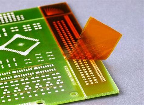
What is PCB Gold Plating?
PCB gold plating is a process of depositing a thin layer of gold onto specific areas of a printed circuit board (PCB). This selective plating technique is used to enhance the conductivity, durability, and corrosion resistance of critical contact points on the PCB, such as connectors, edge contacts, and high-frequency signal traces.
Gold is an excellent choice for plating due to its superior electrical conductivity, resistance to oxidation, and ability to form reliable electrical connections. By selectively applying gold plating to specific areas of the PCB, manufacturers can improve the performance and longevity of the board while minimizing the cost associated with using gold.
Benefits of Selective Gold Plating on PCBs
1. Enhanced Conductivity
Gold is one of the most conductive metals, making it an ideal choice for plating critical contact points on a PCB. By applying a thin layer of gold to these areas, the electrical conductivity is significantly improved, reducing resistance and ensuring reliable signal transmission.
2. Corrosion Resistance
Gold is highly resistant to corrosion and oxidation, which can degrade the performance of electrical contacts over time. By selectively plating gold on exposed contact points, the PCB is protected from environmental factors that can lead to corrosion, ensuring long-term reliability and functionality.
3. Improved Durability
Gold-plated contact points are more durable and resistant to wear compared to unplated surfaces. This is particularly important for PCBs that are subject to frequent insertion and removal cycles, such as connectors and edge contacts. The gold plating helps to minimize wear and tear, extending the lifespan of the PCB.
4. Better Signal Integrity
In high-frequency applications, signal integrity is crucial. Gold-plated signal traces and contact points help to reduce signal loss and maintain signal integrity by minimizing resistance and ensuring reliable electrical connections.
5. Cost-Effective Solution
While gold is a relatively expensive metal, selective gold plating allows manufacturers to leverage its benefits while minimizing costs. By applying gold only to critical areas of the PCB, the overall cost of the board is reduced compared to full gold plating, making it a cost-effective solution for improving PCB performance.

Selective Gold Plating Process
The selective gold plating process involves several steps to ensure accurate and consistent plating on the desired areas of the PCB.
1. PCB Design and Preparation
The first step in the selective gold plating process is to design the PCB layout, specifying the areas that require gold plating. The design files are then used to create a plating mask, which is a template that exposes only the areas to be plated while protecting the rest of the board.
2. Surface Preparation
Before plating can begin, the PCB surface must be thoroughly cleaned to remove any contaminants, such as dirt, grease, or oxidation. This typically involves a combination of chemical cleaning and mechanical abrasion to ensure a clean and uniform surface for plating.
3. Applying the Plating Mask
The plating mask is applied to the PCB, covering the areas that do not require gold plating. This mask is typically made of a photoresist material that is patterned using photolithography. The exposed areas of the PCB are then ready for plating.
4. Electroplating Process
The selective gold plating process typically uses an electroplating method. The PCB is immersed in a gold plating solution, which contains gold ions. An electrical current is applied, causing the gold ions to migrate and adhere to the exposed areas of the PCB. The thickness of the gold layer can be controlled by adjusting the current and plating time.
5. Mask Removal and Cleaning
After the gold plating is complete, the plating mask is removed using a chemical stripper. The PCB is then thoroughly cleaned to remove any residue from the plating process.
6. Inspection and Quality Control
The final step in the selective gold plating process is inspection and quality control. The PCB is visually inspected for any defects or inconsistencies in the gold plating. Electrical tests may also be performed to ensure that the plated areas meet the required specifications for conductivity and signal integrity.

Factors Affecting Selective Gold Plating Quality
Several factors can influence the quality and performance of selective gold plating on PCBs.
1. Gold Purity
The purity of the gold used in the plating process can affect the conductivity and durability of the plated areas. Higher purity gold, such as 99.9% or greater, is typically used for critical applications that require maximum performance and reliability.
2. Plating Thickness
The thickness of the gold plating layer can impact its effectiveness in protecting the underlying surface and providing reliable electrical connections. Typical gold plating thicknesses range from 0.05 to 2.5 microns (2 to 100 microinches), depending on the specific application requirements.
| Application | Typical Gold Plating Thickness |
|---|---|
| Edge Connectors | 0.75 – 1.5 µm (30 – 60 µin) |
| Contact Fingers | 0.75 – 1.5 µm (30 – 60 µin) |
| High-Frequency Signal Traces | 0.05 – 0.25 µm (2 – 10 µin) |
| Wire Bonding Pads | 0.25 – 2.5 µm (10 – 100 µin) |
3. Surface Preparation
Proper surface preparation is essential for achieving a uniform and adherent gold plating layer. Any contaminants or surface imperfections can lead to plating defects, such as voids, nodules, or poor adhesion.
4. Plating Bath Composition
The composition of the gold plating bath, including the concentration of gold ions, pH, and additives, can affect the quality and appearance of the plated layer. Proper maintenance and control of the plating bath are essential for consistent results.
5. Current Density
The current density used during the electroplating process can influence the plating rate, uniformity, and grain structure of the gold layer. Optimal current density values depend on the specific plating bath composition and desired plating thickness.

Applications of Selective Gold Plating on PCBs
Selective gold plating finds applications in various industries where high reliability, conductivity, and durability are essential.
1. Aerospace and Defense
PCBs used in aerospace and defense applications often require selective gold plating to ensure reliable operation in harsh environments, including exposure to extreme temperatures, vibration, and moisture.
2. Automotive Electronics
In automotive electronics, selective gold plating is used on PCB Connectors and high-frequency signal traces to enhance conductivity and protect against corrosion in the demanding under-hood environment.
3. Medical Devices
Medical device PCBs, particularly those used in implantable devices, rely on selective gold plating to provide biocompatibility, corrosion resistance, and reliable electrical connections.
4. Industrial Electronics
Selective gold plating is used in industrial electronics applications to improve the durability and reliability of PCBs exposed to harsh environmental conditions, such as high humidity, temperature fluctuations, and corrosive atmospheres.
5. Consumer Electronics
In consumer electronics, selective gold plating is used on PCB connectors and high-frequency signal traces to ensure reliable connectivity and signal integrity in devices such as smartphones, tablets, and wearables.
Frequently Asked Questions (FAQ)
1. What is the difference between selective gold plating and full gold plating on PCBs?
Selective gold plating involves applying a thin layer of gold only to specific areas of the PCB, such as connectors, edge contacts, and high-frequency signal traces. Full gold plating, on the other hand, covers the entire surface of the PCB with a layer of gold. Selective gold plating is more cost-effective and targeted, while full gold plating provides comprehensive protection and conductivity.
2. How does selective gold plating improve PCB performance?
Selective gold plating improves PCB performance by enhancing the conductivity and durability of critical contact points, protecting against corrosion, and maintaining signal integrity in high-frequency applications.
3. What is the typical thickness of gold plating on PCBs?
The typical thickness of gold plating on PCBs ranges from 0.05 to 2.5 microns (2 to 100 microinches), depending on the specific application requirements. For example, edge connectors and contact fingers typically have a gold plating thickness of 0.75 to 1.5 microns (30 to 60 microinches).
4. Can selective gold plating be applied to any type of PCB?
Selective gold plating can be applied to most types of PCBs, including rigid, flexible, and rigid-flex boards. However, the specific plating process and parameters may need to be adjusted based on the PCB material, design, and application requirements.
5. How does selective gold plating compare to other plating options, such as nickel or silver?
Gold plating offers superior conductivity, corrosion resistance, and durability compared to nickel and silver plating. However, gold is also more expensive than these alternatives. Nickel plating is often used as an undercoat for gold plating to improve adhesion and durability, while silver plating is sometimes used as a more cost-effective option for applications that do not require the same level of performance as gold plating.
In conclusion, selective gold plating is a valuable technique for enhancing the performance, reliability, and longevity of critical areas on PCBs. By understanding the selective gold plating process, factors affecting plating quality, and its applications across various industries, PCB designers and manufacturers can make informed decisions when incorporating selective gold plating into their projects.
No responses yet