What is Microstrip in PCB Design?
Microstrip is a type of electrical transmission line used in printed circuit boards (PCBs) for routing radio frequency (RF) signals. It consists of a conducting strip separated from a ground plane by an insulating dielectric layer.
Some key characteristics of microstrip:
- Unbalanced transmission line
- Quasi-TEM mode of propagation
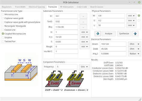
- Impedance determined by width of trace and height of dielectric
- Supports single-ended signaling
- Cheaper to fabricate than stripline
- More susceptible to crosstalk and EMI compared to stripline
Advantages of Microstrip
- Lower fabrication cost compared to stripline
- Supports many types of surface mount components
- Easier to assemble than stripline
- Allows for smaller form factors than stripline
Disadvantages of Microstrip
- Higher radiation and EMI interference compared to stripline
- More susceptible to crosstalk between signals
- Requires precise impedance control
- Can have higher attenuation than stripline at higher frequencies
What is Stripline in PCB Design?
Stripline is a transmission line medium used in multilayer PCBs where the trace is isolated between two ground planes. The two ground planes provide shielding and allow stripline to have excellent noise immunity.
Some key characteristics of stripline:
- Balanced transmission line
- TEM mode of propagation
- Impedance determined by width of trace, height of dielectric, and dielectric constant
- Supports differential signaling
- More expensive to fabricate than microstrip
- Excellent immunity to crosstalk and EMI
Advantages of Stripline
- Excellent noise immunity and minimal crosstalk
- Supports differential signaling
- Lower attenuation than microstrip at higher frequencies
- Minimal radiation and EMI emissions
Disadvantages of Stripline
- Higher fabrication cost compared to microstrip
- Requires at least 3 PCB layers (2 ground planes + signal layer)
- More difficult to assemble surface mount components
- Larger board area required compared to microstrip

What is Coplanar Waveguide (CPW) in PCB Design?
Coplanar waveguide (CPW) is a type of electrical planar transmission line which can be fabricated using printed circuit board technology. It consists of a center strip conductor with semi-infinite ground planes on either side.
Some key characteristics of CPW:
- Uniplanar geometry with signal and grounds on same side of substrate
- Quasi-TEM mode of propagation
- Impedance determined by width of center conductor, gap between conductor and ground planes, and dielectric constant
- Supports single-ended and differential signaling
- Low dispersion up to higher frequencies compared to microstrip
- Allows easy shunt and series connection of components
Advantages of CPW
- Allows smaller dimensions compared to microstrip and stripline
- Lower dispersion than microstrip up to higher frequencies
- Easier integration of lumped and active components
- Supports both single-ended and differential signaling
- Less sensitive to substrate thickness variations
Disadvantages of CPW
- Requires precise fabrication of conductor width and gaps
- Higher conductive losses than microstrip and stripline
- Propagation mode can become non-TEM at higher frequencies
- Requires more metal coverage on PCB

Comparison of Microstrip vs Stripline vs CPW
Here is a comparison table summarizing the key differences between microstrip, stripline, and CPW:
| Property | Microstrip | Stripline | CPW |
|---|---|---|---|
| Trace Geometry | Trace on top or bottom layer | Trace embedded between two ground planes | Center conductor with coplanar ground planes |
| Impedance Control | Moderate | Excellent | Moderate |
| Fabrication Cost | Lowest | Highest | Moderate |
| EMI/Crosstalk | Highest | Lowest | Moderate |
| Radiation Loss | Higher | Minimal | Moderate |
| Circuit Density | Moderate | Lowest | Highest |
| Suitable Frequency Range | Low to moderate | Moderate to high | Low to high |
| Via Usage | High | Low | Low |
The choice between microstrip, stripline, and CPW depends on various factors such as:
- Frequency of operation
- Required impedance
- Number of PCB layers available
- Allowable radiation and EMI
- Component types and density
- Cost constraints
In general, microstrip is a good choice for low cost, lower frequency designs where some EMI is acceptable. Stripline provides the best noise immunity and signal integrity at the cost of higher fabrication complexity and cost. CPW allows high density circuits and easy integration of components at the expense of higher losses.

Microstrip PCB Design Guidelines
Here are some key guidelines to follow when designing microstrip PCBs:
-
Choose appropriate substrate material based on dielectric constant and loss tangent requirements. Common choices are FR-4, Rogers 4003, Rogers 5870.
-
Determine the characteristic impedance and trace dimensions using a microstrip impedance calculator. Typical impedances are 50Ω, 75Ω, and 100Ω.
-
Maintain a constant trace width and spacing to preserve impedance along the transmission line. Avoid abrupt bends and use mitered corners for 90° turns.
-
Provide sufficient clearance between microstrip traces to minimize crosstalk. A minimum spacing of 3W between traces is recommended, where W is the trace width.
-
Use ground pour on the same layer as the microstrip trace and stitch it to the bottom ground plane with vias. This helps reduce radiation and provides consistent return path.
-
Avoid routing microstrip traces near board edges or gaps in the ground plane, as this can cause discontinuities and reflections.
-
Use smooth transitions when changing layers, such as tapered lines or curved bends. Abrupt transitions can cause impedance mismatch and reflections.
-
Keep microstrip traces short to minimize losses, especially at high frequencies. Use components with minimal parasitic inductance and capacitance.
-
Consider using a soldermask coating over the microstrip traces to protect against oxidation and contamination.
-
Perform signal integrity simulations to verify the microstrip design and optimize terminations, layout, and stack-up as needed.
Following these guidelines can help ensure reliable performance of microstrip transmission lines in your PCB design.
Frequently Asked Questions
1. What is the difference between microstrip and stripline?
Microstrip has the signal trace on the top or bottom layer of the PCB, while stripline has the signal trace embedded between two ground planes. Microstrip is easier to fabricate but has higher EMI and crosstalk, while stripline provides better noise immunity but is more expensive.
2. Can I use microstrip for high-speed digital signals?
Yes, microstrip can be used for high-speed digital signals up to a few GHz. However, at higher frequencies, the dispersion and losses of microstrip can degrade signal integrity. Stripline or CPW may be better suited for very high-speed signals.
3. How do I choose the right impedance for my microstrip trace?
The characteristic impedance of a microstrip trace depends on the trace width, dielectric thickness, and dielectric constant of the substrate. Use a microstrip impedance calculator to determine the required trace width for your desired impedance. Common impedances are 50Ω, 75Ω, and 100Ω.
4. What is the best way to route a microstrip trace on a PCB?
When routing microstrip traces, try to maintain a constant trace width and spacing to preserve impedance. Avoid abrupt bends and use mitered corners for 90° turns. Provide sufficient clearance between traces to minimize crosstalk, and avoid routing near board edges or gaps in the ground plane.
5. Can I mix microstrip and stripline on the same PCB?
Yes, it is possible to use both microstrip and stripline on the same PCB. This can be useful for routing signals with different requirements, such as low-speed control signals on microstrip and high-speed data signals on stripline. However, be sure to use appropriate transitions when changing between the two types of transmission lines to avoid impedance mismatches and reflections.
No responses yet