Introduction to EMC PCB Design
Electromagnetic Compatibility (EMC) is a critical aspect of printed circuit board (PCB) design that ensures electronic devices can function properly in their intended electromagnetic environment without causing or being susceptible to electromagnetic interference (EMI). Proper EMC PCB Design is essential to meet EMC standards and regulations, ensure the reliability and performance of electronic devices, and avoid costly redesigns and compliance issues.
In this Comprehensive Guide, we will delve into the principles of EMC PCB design, discuss key EMC standards, and provide best practices and techniques to achieve EMC compliance in your PCB designs.
Understanding Electromagnetic Interference (EMI)
EMI is the disruption of the normal operation of an electronic device due to unintended electromagnetic emissions from another device or source. There are two main types of EMI:
- Conducted EMI: Interference that propagates through conductive paths such as power lines, signal traces, or ground planes.
- Radiated EMI: Interference that propagates through the air as electromagnetic waves, either from the device itself or from external sources.
To mitigate EMI, it is crucial to understand the sources of EMI and the mechanisms by which it can couple into a PCB or electronic device.
Common Sources of EMI
- Switching power supplies
- High-speed digital circuits
- Electrostatic discharge (ESD)
- Lightning strikes
- Radio frequency (RF) transmitters
- Electric motors and generators
EMI Coupling Mechanisms
- Conducted coupling: EMI propagates through shared conductive paths, such as power lines or ground planes.
- Capacitive coupling: EMI couples between adjacent conductors through electric fields.
- Inductive coupling: EMI couples between conductors through magnetic fields.
- Radiated coupling: EMI propagates through the air as electromagnetic waves and couples into the device through apertures or antenna-like structures.

Key Principles of EMC PCB Design
To achieve EMC compliance and minimize EMI, follow these key principles in your PCB designs:
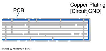
1. Grounding and Shielding
Proper grounding and shielding are essential for controlling EMI. Use the following techniques:
- Implement a low-impedance ground plane to provide a stable reference for signals and minimize ground loops.
- Use shield cans or conductive enclosures to contain EMI from high-noise components.
- Employ proper cable shielding and terminate shields to the ground plane.
2. Power Distribution Network (PDN) Design
A well-designed PDN is crucial for minimizing conducted EMI and ensuring clean power delivery to components. Consider these guidelines:
- Use decoupling capacitors close to ICs to suppress high-frequency noise.
- Implement power plane segmentation to isolate noisy circuits from sensitive ones.
- Employ ferrite beads or EMI filters to suppress conducted EMI on power lines.
3. Signal Integrity and Trace Routing
Proper signal integrity and trace routing techniques can help minimize radiated EMI and crosstalk. Follow these best practices:
- Keep high-speed traces as short as possible and avoid unnecessary layer transitions.
- Route sensitive traces away from noisy components and traces.
- Use differential signaling for high-speed interfaces to minimize EMI.
- Terminate traces properly to avoid reflections and ringing.
4. Component Placement and Layout
Strategic component placement and layout can help control EMI and improve EMC performance. Consider these tips:
- Group components based on their noise levels and sensitivity.
- Place noisy components, such as switching regulators, away from sensitive analog circuits.
- Minimize the loop area of high-current paths to reduce magnetic field coupling.
- Orient components to minimize coupling and provide natural shielding.
5. Filtering and Suppression Techniques
Incorporate filtering and suppression techniques to attenuate EMI at its source or prevent it from propagating. Some common methods include:
- Use EMI filters on power lines and I/O interfaces.
- Implement Snubber Circuits or transient voltage suppressors (TVS) to reduce high-frequency noise and voltage spikes.
- Employ common-mode chokes or ferrite beads to suppress common-mode EMI.

EMC Standards and Regulations
To ensure EMC compliance, it is essential to understand and adhere to relevant EMC standards and regulations. Some key EMC standards include:
FCC Part 15 (USA)
- Regulates emissions from digital devices to prevent interference with radio communications.
- Classifies devices into Class A (industrial) and Class B (residential) based on their intended use and emission limits.
CISPR 22 and CISPR 32 (International)
- CISPR 22 defines limits and methods for measuring radiated and conducted emissions from information technology equipment (ITE).
- CISPR 32 is an updated version of CISPR 22 that covers multimedia equipment.
IEC 61000-4 Series (International)
- Defines immunity requirements and test methods for various electromagnetic phenomena, such as ESD, radiated RF fields, and conducted disturbances.
MIL-STD-461 (Military)
- Specifies EMC requirements for military and aerospace equipment.
- Covers both emissions and susceptibility tests for various electromagnetic environments.
It is crucial to consult the specific standards and regulations applicable to your industry and target market to ensure compliance.

EMC Testing and Compliance
To verify EMC compliance, it is necessary to perform EMC testing on your PCB or electronic device. EMC testing typically involves two main categories:
-
Emissions testing: Measures the electromagnetic emissions generated by the device to ensure they are within the limits specified by relevant standards.
-
Immunity testing: Evaluates the device’s ability to function properly in the presence of electromagnetic disturbances, such as ESD, radiated RF fields, and conducted disturbances.
EMC testing should be performed in an accredited EMC testing laboratory that adheres to standardized test methods and procedures. It is recommended to engage with an EMC testing lab early in the design process to identify potential EMC issues and minimize the risk of compliance failures.
Best Practices for EMC PCB Design
To summarize, here are some best practices to follow for successful EMC PCB design:
- Start considering EMC early in the design process to avoid costly redesigns and delays.
- Understand the EMC standards and regulations applicable to your product and target market.
- Follow good grounding and shielding practices to control EMI.
- Design a robust power distribution network with proper decoupling and filtering.
- Implement proper signal integrity and trace routing techniques to minimize radiated EMI and crosstalk.
- Strategically place and orient components to control EMI and improve EMC performance.
- Incorporate filtering and suppression techniques to attenuate EMI at its source or prevent propagation.
- Perform pre-compliance EMC testing to identify and address potential issues early in the design process.
- Engage with an accredited EMC testing laboratory to ensure compliance with relevant standards.
- Document your EMC design decisions and test results for future reference and continuous improvement.
Frequently Asked Questions (FAQ)
1. What is the difference between EMC and EMI?
EMC (Electromagnetic Compatibility) refers to the ability of an electronic device to function properly in its intended electromagnetic environment without causing or being susceptible to EMI (Electromagnetic Interference). EMI is the actual disruption or degradation of the performance of an electronic device due to electromagnetic emissions from another device or source.
2. Why is EMC important in PCB design?
EMC is crucial in PCB design to ensure that electronic devices can function reliably and safely in their intended electromagnetic environment. Proper EMC design helps to:
– Prevent interference with other electronic devices
– Avoid susceptibility to external electromagnetic disturbances
– Meet regulatory requirements and standards
– Minimize the risk of costly redesigns and compliance issues
3. What are the main types of EMI coupling in PCBs?
The main types of EMI coupling in PCBs are:
– Conducted coupling: EMI propagates through shared conductive paths, such as power lines or ground planes.
– Capacitive coupling: EMI couples between adjacent conductors through electric fields.
– Inductive coupling: EMI couples between conductors through magnetic fields.
– Radiated coupling: EMI propagates through the air as electromagnetic waves and couples into the device through apertures or antenna-like structures.
4. How can I minimize radiated EMI in my PCB design?
To minimize radiated EMI in your PCB design, follow these techniques:
– Keep high-speed traces as short as possible and avoid unnecessary layer transitions.
– Route sensitive traces away from noisy components and traces.
– Use differential signaling for high-speed interfaces.
– Terminate traces properly to avoid reflections and ringing.
– Implement proper grounding and shielding practices.
– Strategically place and orient components to control EMI.
5. What should I do if my device fails EMC compliance testing?
If your device fails EMC compliance testing, take the following steps:
1. Analyze the test results to identify the specific EMC issues and their root causes.
2. Review your EMC design and identify areas for improvement based on the test results and EMC best practices.
3. Implement necessary design changes, such as improved grounding, shielding, filtering, or trace routing.
4. Perform pre-compliance testing to verify the effectiveness of the design changes.
5. Re-submit the device for compliance testing at an accredited EMC testing laboratory.
6. Document the design changes and test results for future reference and continuous improvement.
Conclusion
EMC PCB design is a critical aspect of electronic product development that ensures devices can function reliably and safely in their intended electromagnetic environment. By understanding the principles of EMC, following best practices in PCB design, and adhering to relevant EMC standards and regulations, you can minimize EMI, improve EMC performance, and avoid costly compliance issues.
Remember to start considering EMC early in the design process, engage with EMC experts and testing laboratories, and continuously improve your EMC design practices based on test results and industry advancements.
| Aspect | Description |
|---|---|
| EMI Types | Conducted EMI, Radiated EMI |
| EMI Coupling Mechanisms | Conducted coupling, Capacitive coupling, Inductive coupling, Radiated coupling |
| Key EMC Design Principles | Grounding and shielding, Power distribution network design, Signal integrity and trace routing, Component placement and layout, Filtering and suppression techniques |
| Common EMC Standards | FCC Part 15 (USA), CISPR 22 and CISPR 32 (International), IEC 61000-4 Series (International), MIL-STD-461 (Military) |
| EMC Testing Categories | Emissions testing, Immunity testing |
By following this comprehensive guide and implementing the techniques and best practices discussed, you can navigate the complex landscape of EMC PCB design and ensure your electronic devices meet the necessary EMC standards and perform reliably in their intended electromagnetic environment.
No responses yet