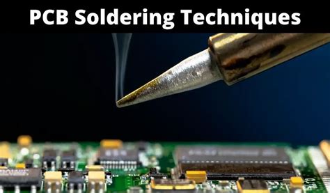
Introduction to PCB Soldering
Printed Circuit Board (PCB) soldering is a crucial process in the manufacturing of electronic devices. It involves the attachment of electronic components to the PCB using a molten metal alloy called solder. The soldering process ensures a strong mechanical bond and excellent electrical connectivity between the components and the PCB.
PCB soldering is a complex process that requires precision, skill, and the right equipment. There are various types of PCB soldering techniques, each with its advantages and disadvantages. In this article, we will explore the different types of PCB soldering and assembly processes.
Types of PCB Soldering
Through-Hole Soldering
Through-hole soldering is one of the oldest and most reliable methods of PCB soldering. In this technique, the electronic components have long leads that are inserted into holes drilled on the PCB. The leads are then soldered to the copper pads on the opposite side of the board.
Advantages of through-hole soldering:
– Strong mechanical bond
– Easy to inspect and repair
– Suitable for high-power applications
Disadvantages of through-hole soldering:
– Time-consuming process
– Requires more space on the PCB
– Not suitable for high-density designs
Surface Mount Soldering
Surface Mount Technology (SMT) is a modern PCB soldering technique that has gained popularity in recent years. In this method, the electronic components are placed directly on the surface of the PCB and soldered using a solder paste.
Advantages of surface mount soldering:
– Faster assembly process
– Allows for high-density designs
– Suitable for automated assembly
Disadvantages of surface mount soldering:
– Requires specialized equipment
– Difficult to inspect and repair
– Not suitable for high-power applications
Wave Soldering
Wave soldering is an automated PCB soldering process that is used for through-hole components. In this technique, the PCB is passed over a molten solder wave, which coats the copper pads and component leads with solder.
Advantages of wave soldering:
– Fast and efficient process
– Suitable for high-volume production
– Provides a strong mechanical bond
Disadvantages of wave soldering:
– Not suitable for surface mount components
– Can cause thermal stress on the PCB
– Requires specialized equipment
Reflow Soldering
Reflow soldering is an automated PCB soldering process that is used for surface mount components. In this technique, a solder paste is applied to the PCB using a stencil, and the components are placed on top of the paste. The PCB is then passed through a reflow oven, which melts the solder paste and bonds the components to the board.
Advantages of reflow soldering:
– Fast and efficient process
– Suitable for high-volume production
– Provides a strong mechanical bond
Disadvantages of reflow soldering:
– Requires specialized equipment
– Can cause thermal stress on the PCB
– Not suitable for through-hole components
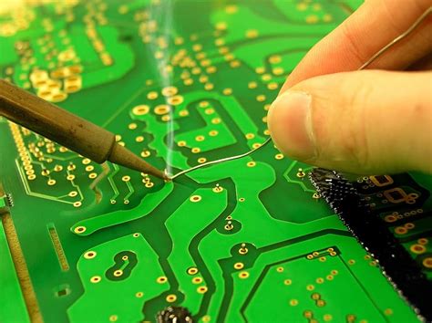
Hand Soldering
Hand soldering is a manual PCB soldering process that is used for small-scale production or prototyping. In this technique, a soldering iron is used to apply solder to the component leads and PCB pads.
Advantages of hand soldering:
– Low cost and simple process
– Suitable for small-scale production or prototyping
– Allows for precise control over the soldering process
Disadvantages of hand soldering:
– Time-consuming process
– Requires skilled operators
– Not suitable for high-volume production

PCB Assembly Processes
Surface Mount Assembly (SMT)
Surface Mount Assembly (SMT) is an automated PCB assembly process that involves placing surface mount components on the PCB using a pick-and-place machine. The components are then soldered to the board using reflow soldering.
Advantages of SMT assembly:
– Fast and efficient process
– Suitable for high-volume production
– Allows for high-density designs
Disadvantages of SMT assembly:
– Requires specialized equipment
– Can be expensive for small-scale production
– Difficult to inspect and repair
Through-Hole Assembly (THA)
Through-Hole Assembly (THA) is a manual PCB assembly process that involves inserting through-hole components into the holes on the PCB and soldering them using wave soldering.
Advantages of THA assembly:
– Strong mechanical bond
– Suitable for high-power applications
– Easy to inspect and repair
Disadvantages of THA assembly:
– Time-consuming process
– Requires more space on the PCB
– Not suitable for high-density designs
Mixed Technology Assembly (MTA)
Mixed Technology Assembly (MTA) is a PCB assembly process that involves combining surface mount and through-hole components on the same PCB. This process requires a combination of SMT and THA assembly techniques.
Advantages of MTA assembly:
– Allows for a wider range of component types
– Provides a strong mechanical bond
– Suitable for complex designs
Disadvantages of MTA assembly:
– Requires specialized equipment
– Can be expensive and time-consuming
– Difficult to inspect and repair

PCB Soldering and Assembly Process Flow
The PCB soldering and assembly process typically follows these steps:
- PCB Design and Fabrication
- Solder Paste Application (for SMT)
- Component Placement
- Soldering (Reflow or Wave)
- Inspection and Testing
- Rework and Repair (if necessary)
- Conformal Coating (optional)
- Final Assembly and Packaging
| Step | SMT Process | THA Process |
|---|---|---|
| 1 | PCB Design and Fabrication | PCB Design and Fabrication |
| 2 | Solder Paste Application | Component Placement |
| 3 | Component Placement | Soldering (Wave) |
| 4 | Soldering (Reflow) | Inspection and Testing |
| 5 | Inspection and Testing | Rework and Repair (if necessary) |
| 6 | Rework and Repair (if necessary) | Conformal Coating (optional) |
| 7 | Conformal Coating (optional) | Final Assembly and Packaging |
| 8 | Final Assembly and Packaging | – |
Factors Affecting PCB Soldering Quality
Several factors can affect the quality of PCB soldering, including:
- Solder alloy composition
- Soldering temperature and time
- Flux type and activity
- PCB and component cleanliness
- Operator skill and experience
- Environmental conditions (humidity, temperature, etc.)
To ensure high-quality PCB soldering, it is important to control these factors and follow best practices for each soldering technique.
Inspection and Testing of Soldered PCBs
After the soldering process, it is important to inspect and test the PCBs to ensure that they meet the required quality standards. Some common inspection and testing methods include:
- Visual inspection
- X-ray inspection
- In-circuit testing (ICT)
- Functional testing
- Boundary scan testing
These methods help identify any defects or issues with the soldered PCBs, such as bridging, poor wetting, or component misalignment.
Rework and Repair of Soldered PCBs
Despite best efforts, sometimes soldered PCBs may require rework or repair due to defects or issues identified during inspection and testing. Rework and repair involve removing the defective component or solder joint and replacing it with a new one.
Some common rework and repair techniques include:
– Desoldering and resoldering
– Component replacement
– Solder joint repair
– Trace repair
Rework and repair can be time-consuming and expensive, so it is important to minimize the need for them by ensuring high-quality soldering and assembly processes.
Conformal Coating of Soldered PCBs
Conformal coating is an optional step in the PCB assembly process that involves applying a protective layer over the soldered PCB. The coating helps protect the PCB from environmental factors such as moisture, dust, and chemicals.
Some common conformal coating materials include:
– Acrylic
– Silicone
– Polyurethane
– Epoxy
Conformal coating can be applied using various methods, such as spraying, dipping, or brushing, depending on the specific requirements of the PCB and the coating material.
Final Assembly and Packaging
The final step in the PCB assembly process is the assembly and packaging of the finished product. This involves integrating the soldered PCB with other components, such as connectors, cables, and enclosures, to create the final product.
The packaging process involves protecting the finished product during storage and transportation, using materials such as antistatic bags, foam inserts, and corrugated boxes.
Conclusion
PCB soldering and assembly is a complex process that requires precision, skill, and the right equipment. There are various types of PCB soldering and assembly techniques, each with its advantages and disadvantages. Choosing the right technique depends on factors such as the PCB design, component types, and production volume.
To ensure high-quality PCB soldering and assembly, it is important to control the various factors that can affect the process, such as solder alloy composition, soldering temperature and time, and operator skill and experience. Inspection and testing, rework and repair, and conformal coating are also important steps in the PCB assembly process.
By understanding the different types of PCB soldering and assembly processes and following best practices, manufacturers can produce high-quality, reliable electronic products that meet the required specifications and standards.
Frequently Asked Questions (FAQ)
- What is the difference between through-hole and surface mount soldering?
-
Through-hole soldering involves inserting component leads into holes drilled on the PCB and soldering them on the opposite side, while surface mount soldering involves placing components directly on the surface of the PCB and soldering them using a solder paste.
-
What are the advantages of surface mount soldering over through-hole soldering?
-
Surface mount soldering allows for faster assembly, higher component density, and automated assembly processes, while through-hole soldering provides a stronger mechanical bond and is easier to inspect and repair.
-
What is the purpose of solder flux in PCB soldering?
-
Solder flux is a chemical agent that helps remove oxides and other contaminants from the surfaces to be soldered, promoting better wetting and bonding of the solder to the metal surfaces.
-
What is the difference between reflow and wave soldering?
-
Reflow soldering is used for surface mount components and involves applying a solder paste to the PCB and melting it in a reflow oven, while wave soldering is used for through-hole components and involves passing the PCB over a molten solder wave.
-
What are some common defects that can occur during PCB soldering?
- Some common defects in PCB soldering include bridging (solder connecting adjacent pins), poor wetting (solder not adhering properly to the metal surfaces), solder balls (small spheres of solder that can cause short circuits), and component misalignment.
No responses yet