Introduction to PCB Stackups
In the world of printed circuit board (PCB) design, the stackup refers to the arrangement of copper and insulating layers that make up the board. The choice of stackup is crucial as it directly impacts the electrical performance, signal integrity, and manufacturability of the PCB. When designing high-speed digital circuits or RF systems, maintaining a consistent characteristic impedance, such as 50 ohms, is essential for optimal signal transmission and minimizing reflections.
In this article, we will explore two alternative 4-layer PCB stackups that can achieve a 50-ohm impedance. We will discuss the advantages and disadvantages of each stackup, the materials used, and the design considerations for ensuring a robust and reliable PCB.
Understanding Characteristic Impedance
Before diving into the stackup alternatives, let’s briefly discuss characteristic impedance. Characteristic impedance is the resistance to the propagation of an electrical signal along a transmission line, such as a PCB trace. It is determined by the geometry of the trace, the dielectric properties of the surrounding materials, and the frequency of the signal.
For a microstrip trace (a trace on the outer layer of the PCB), the characteristic impedance is given by:
Z0 = 87 / √(εr + 1.41) * ln(5.98 * h / (0.8 * w + t))
Where:
– Z0 is the characteristic impedance in ohms
– εr is the relative dielectric constant of the substrate material
– h is the height of the substrate between the trace and the reference plane
– w is the width of the trace
– t is the thickness of the trace
For a stripline trace (a trace embedded between two reference planes), the characteristic impedance is given by:
Z0 = 60 / √εr * ln(4 * h / (0.67 * π * (0.8 * w + t)))
Where the variables have the same meaning as in the microstrip equation.
To achieve a 50-ohm characteristic impedance, we need to carefully select the substrate material, trace dimensions, and layer thicknesses in our PCB stackup.
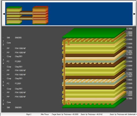
4 Layer PCB Stackup Alternative 1: FR4 with Thin Dielectric
The first alternative for a 4-layer PCB stackup with 50-ohm impedance uses FR4 as the substrate material and employs a thin dielectric layer between the signal and reference planes.
Layer Stack
| Layer | Material | Thickness (mil) | Copper Weight (oz) |
|---|---|---|---|
| Top | FR4 | 1.7 | 1 |
| Ground | FR4 | 4.7 | 0.5 |
| Power | FR4 | 4.7 | 0.5 |
| Bottom | FR4 | 1.7 | 1 |
In this stackup, the top and bottom layers are used for signal routing, while the inner layers serve as ground and power planes. The total thickness of the board is approximately 62 mils (1.57 mm).
Advantages
- FR4 is a widely available and cost-effective substrate material.
- The thin dielectric layer between the signal and reference planes allows for tighter coupling, which helps maintain a consistent characteristic impedance.
- The symmetrical stackup balances the mechanical stresses, reducing warpage.
Disadvantages
- The thin dielectric layer may increase the manufacturing complexity and cost.
- The reduced spacing between layers may lead to higher crosstalk and signal integrity issues if not properly designed.
Design Considerations
- Use appropriate trace widths and spacing to achieve the desired impedance. For this stackup, a trace width of approximately 7 mils and a spacing of 7 mils between traces can yield a 50-ohm microstrip impedance.
- Ensure proper grounding and power distribution to minimize noise and interference.
- Follow the manufacturer’s design rules and guidelines for minimum trace widths, spacings, and via sizes.

4 Layer PCB Stackup Alternative 2: Low-Loss Material with Thicker Dielectric
The second alternative for a 4-layer PCB stackup with 50-ohm impedance uses a low-loss material, such as Rogers RO4350B, as the substrate and employs a thicker dielectric layer between the signal and reference planes.
Layer Stack
| Layer | Material | Thickness (mil) | Copper Weight (oz) |
|---|---|---|---|
| Top | RO4350B | 3.6 | 1 |
| Ground | RO4350B | 14.7 | 0.5 |
| Power | RO4350B | 14.7 | 0.5 |
| Bottom | RO4350B | 3.6 | 1 |
In this stackup, the top and bottom layers are used for signal routing, while the inner layers serve as ground and power planes. The total thickness of the board is approximately 107 mils (2.72 mm).
Advantages
- Low-loss materials, such as RO4350B, have a lower dielectric constant and dissipation factor, which reduces signal attenuation and improves signal integrity.
- The thicker dielectric layer provides better isolation between layers, reducing crosstalk and electromagnetic interference (EMI).
- The symmetrical stackup balances the mechanical stresses, reducing warpage.
Disadvantages
- Low-loss materials are more expensive than FR4, increasing the overall cost of the PCB.
- The thicker dielectric layer may increase the overall thickness of the board, which may not be suitable for some applications with strict height constraints.
Design Considerations
- Use appropriate trace widths and spacing to achieve the desired impedance. For this stackup, a trace width of approximately 12 mils and a spacing of 12 mils between traces can yield a 50-ohm microstrip impedance.
- Ensure proper grounding and power distribution to minimize noise and interference.
- Follow the manufacturer’s design rules and guidelines for minimum trace widths, spacings, and via sizes.
Comparing the Alternatives
When choosing between the two alternative 4-layer PCB stackups, consider the following factors:
- Cost: The FR4 stackup with a thin dielectric layer is generally more cost-effective than the low-loss material stackup with a thicker dielectric layer.
- Signal integrity: The low-loss material stackup provides better signal integrity and reduced signal attenuation, making it more suitable for high-speed digital circuits or RF applications.
- Board thickness: The FR4 stackup results in a thinner overall board thickness, which may be advantageous for space-constrained designs.
- Manufacturing complexity: The thin dielectric layer in the FR4 stackup may increase manufacturing complexity and cost compared to the thicker dielectric layer in the low-loss material stackup.
Ultimately, the choice between the two alternatives depends on the specific requirements of your project, such as budget, performance, and mechanical constraints.
Frequently Asked Questions (FAQ)
-
Q: Can I achieve a 50-ohm impedance with a different number of layers in my PCB stackup?
A: Yes, it is possible to achieve a 50-ohm impedance with different numbers of layers, such as 2-layer or 6-layer stackups. However, the design complexity and constraints may vary depending on the number of layers and the chosen materials. -
Q: What other substrate materials can be used for a 4-layer PCB stackup with 50-ohm impedance?
A: Apart from FR4 and Rogers RO4350B, other substrate materials that can be used include Isola FR408HR, Isola I-Tera MT40, and Nelco N4000-13SI. The choice of material depends on the specific requirements of your application, such as frequency range, thermal properties, and cost. -
Q: How does the choice of stackup affect the manufacturability of the PCB?
A: The choice of stackup can impact the manufacturability of the PCB in several ways. Thinner dielectric layers may require more precise manufacturing processes and increase the likelihood of defects. Additionally, the choice of substrate material and the number of layers can affect the drilling, plating, and lamination processes, which may impact the overall manufacturing yield and cost. -
Q: Can I mix different substrate materials in a single PCB stackup?
A: Yes, it is possible to mix different substrate materials in a single PCB stackup, known as a hybrid stackup. This approach can be used to optimize the performance and cost of the PCB by using high-performance materials only where necessary and using cost-effective materials elsewhere. However, hybrid stackups may increase the design and manufacturing complexity. -
Q: How can I verify that my PCB stackup achieves the desired 50-ohm impedance?
A: To verify that your PCB stackup achieves the desired 50-ohm impedance, you can use a variety of tools and techniques, such as: - Impedance calculators: Many PCB design software packages include impedance calculators that can estimate the characteristic impedance based on the stackup parameters.
- Field solvers: 2D or 3D field solvers can provide more accurate simulations of the electromagnetic fields and impedances in your PCB stackup.
- Time-domain reflectometry (TDR): TDR measurements can be performed on a manufactured PCB to measure the actual impedance of the traces and verify that they match the desired value.
Conclusion
Choosing the right 4-layer PCB stackup is crucial for achieving a consistent 50-ohm characteristic impedance and ensuring optimal signal integrity in your high-speed digital or RF design. The two alternative stackups presented in this article, one using FR4 with a thin dielectric layer and the other using a low-loss material with a thicker dielectric layer, offer different advantages and trade-offs in terms of cost, performance, and manufacturability.
When selecting a stackup, carefully consider your project’s specific requirements, budget, and constraints. Use appropriate design tools and calculators to validate your stackup choice and ensure that it meets the desired impedance and signal integrity targets. By following best practices and working closely with your PCB manufacturer, you can successfully implement a 4-layer PCB stackup that achieves a 50-ohm impedance and delivers reliable performance in your application.
No responses yet