Introduction to TL494
The TL494 is a versatile and widely used pulse-width modulation (PWM) control circuit. It is designed for power supply control applications, such as switching power supplies, DC-to-DC converters, and battery chargers. The TL494 offers a range of features that make it an attractive choice for many projects, including:
- Wide supply voltage range (7V to 40V)
- Adjustable frequency (up to 300 kHz)
- Dual error amplifiers for voltage and current control
- Deadtime control for push-pull outputs
- Undervoltage lockout and soft-start capability
In this comprehensive guide, we will dive deep into the TL494, exploring its pinout, internal architecture, and various applications. By the end of this article, you will have a solid understanding of how to incorporate the TL494 into your power supply projects.
TL494 Pinout and Function Description
The TL494 comes in a 16-pin DIP or SOIC package. Here’s a detailed description of each pin and its function:
| Pin Number | Pin Name | Description |
|---|---|---|
| 1 | 1IN- | Inverting input of error amplifier 1 |
| 2 | 1IN+ | Non-inverting input of error amplifier 1 |
| 3 | FB | Output of error amplifier 1 |
| 4 | DTC | Deadtime control pin |
| 5 | CT | Oscillator timing capacitor |
| 6 | RT | Oscillator timing resistor |
| 7 | GND | Ground |
| 8 | C1 | Collector of output transistor 1 |
| 9 | E1 | Emitter of output transistor 1 |
| 10 | E2 | Emitter of output transistor 2 |
| 11 | C2 | Collector of output transistor 2 |
| 12 | VCC | Positive supply voltage |
| 13 | Output Control | Output control pin |
| 14 | REF | 5V reference voltage output |
| 15 | 2IN- | Inverting input of error amplifier 2 |
| 16 | 2IN+ | Non-inverting input of error amplifier 2 |
Error Amplifiers
The TL494 features two error amplifiers, each with its own inverting and non-inverting inputs. These amplifiers are used to compare the output voltage or current with a reference value, generating an error signal that is used to control the PWM output.
Oscillator
The oscillator frequency is set by the RT and CT pins. The frequency can be calculated using the following formula:
f = 1 / (R_T * C_T)
where f is the oscillator frequency, R_T is the resistance connected to the RT pin, and C_T is the capacitance connected to the CT pin.
Output Stage
The TL494 has two push-pull output transistors, which can be used to drive a power MOSFET or transformer directly. The deadtime between the two outputs can be adjusted using the DTC pin, which helps prevent shoot-through currents in push-pull configurations.

TL494 Internal Architecture
To better understand how the TL494 works, let’s take a closer look at its internal architecture.
Block Diagram
The TL494 consists of several key components:
-
Error Amplifiers: Two error amplifiers compare the feedback signals with the reference voltage, generating error signals that control the PWM output.
-
Oscillator: A sawtooth oscillator generates the PWM ramp signal, with the frequency determined by the RT and CT pins.
-
Comparators: The error signals from the amplifiers are compared with the sawtooth waveform to generate the PWM output.
-
Output Stage: The push-pull output transistors drive the external power devices, with deadtime control provided by the DTC pin.
-
Reference Voltage: A 5V reference voltage is available at the REF pin for use in feedback networks and other applications.
PWM Operation
The TL494 generates a PWM output by comparing the error signals from the amplifiers with the sawtooth waveform from the oscillator. When the error signal is higher than the sawtooth, the output is turned on, and when the error signal is lower, the output is turned off. The duty cycle of the PWM output is proportional to the error signal, allowing for precise control of the output voltage or current.

TL494 Applications
The TL494 is widely used in various power supply applications, such as:
- DC-to-DC converters: Buck, boost, and buck-Boost Converters
- Switching power supplies: Flyback, forward, and push-pull topologies
- Battery chargers: Lead-acid, lithium-ion, and NiMH battery charging circuits
- Motor speed control: PWM-based motor speed control systems
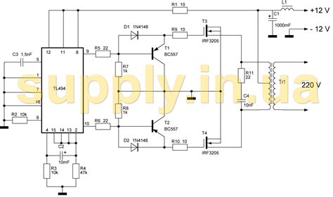
Example: Basic Buck Converter
Here’s an example of a basic buck converter using the TL494:
In this circuit, the TL494 is configured as a voltage-mode controller, with the output voltage feedback connected to the inverting input of error amplifier 1. The error amplifier output controls the PWM duty cycle, which in turn regulates the output voltage. The inductor and capacitor form the output filter, smoothing the PWM waveform into a clean DC voltage.

TL494 Design Considerations
When designing with the TL494, there are several key considerations to keep in mind:
-
Feedback network: Proper design of the feedback network is crucial for stable operation and accurate regulation. Use appropriate compensation techniques, such as type II or type III compensation, to ensure loop stability.
-
Oscillator frequency: Choose an appropriate oscillator frequency based on your application requirements. Higher frequencies allow for smaller inductor and capacitor values but may increase switching losses.
-
Output stage: Ensure that the output transistors are capable of handling the required current and voltage levels. Use external power devices, such as MOSFETs or IGBTs, for higher power applications.
-
PCB layout: Proper PCB layout is essential for minimizing noise and ensuring reliable operation. Keep high-frequency traces short, use appropriate grounding techniques, and provide adequate heatsinking for power components.
TL494 Alternatives
While the TL494 is a popular choice for many power supply applications, there are several alternatives available that offer similar or enhanced features:
- UC3842/3/4/5: A family of PWM controllers with current-mode control and enhanced protection features.
- MC34063: A versatile DC-to-DC converter IC with built-in switch and adjustable frequency.
- LM5035: A high-voltage PWM controller with integrated high-side gate driver and fault protection.
Consider these alternatives when designing your power supply, as they may better suit your specific requirements.
Frequently Asked Questions (FAQ)
-
Q: What is the maximum supply voltage for the TL494?
A: The TL494 can operate with a supply voltage range of 7V to 40V. -
Q: How do I set the oscillator frequency of the TL494?
A: The oscillator frequency is set by the RT and CT pins. Use the formula f = 1 / (R_T * C_T) to calculate the required resistor and capacitor values. -
Q: Can the TL494 be used for current-mode control?
A: While the TL494 is primarily designed for voltage-mode control, it can be adapted for current-mode control by using the second error amplifier to sense the inductor current. -
Q: What is the purpose of the deadtime control (DTC) pin?
A: The DTC pin allows for adjustment of the deadtime between the two output transistors, preventing shoot-through currents in push-pull configurations. -
Q: How do I compensate the feedback loop for stable operation?
A: Use appropriate compensation techniques, such as type II or type III compensation, to ensure loop stability. The compensation network should be designed based on the specific requirements of your application, considering factors such as the oscillator frequency, output filter characteristics, and load range.
Conclusion
The TL494 is a powerful and versatile PWM control circuit that finds applications in a wide range of power supply designs. Its dual error amplifiers, adjustable oscillator frequency, and push-pull output stage make it an attractive choice for DC-to-DC converters, switching power supplies, and battery chargers.
By understanding the TL494’s pinout, internal architecture, and design considerations, you can effectively incorporate this device into your projects. Remember to carefully design your feedback network, choose an appropriate oscillator frequency, and follow best practices for PCB layout to ensure optimal performance and reliability.
As you explore the world of power supply design, consider the TL494 as a valuable tool in your arsenal. With its flexibility and robustness, it can help you bring your power supply projects to life, whether you’re working on a simple buck converter or a complex multi-stage system.
No responses yet