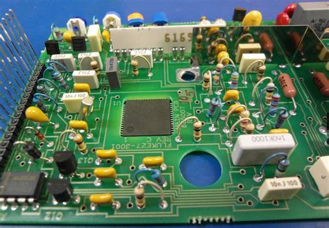
What is Through-Hole Assembly?
Through-hole assembly, also known as through-hole technology (THT), is a method of mounting electronic components on a printed circuit board (PCB) by inserting the component leads through holes drilled in the board and soldering them to pads on the opposite side. This method has been used for decades and remains a reliable and robust way to assemble PCBs, especially for larger components or those subjected to mechanical stress.
Advantages of Through-Hole Assembly
- Mechanical strength: Through-hole components are securely attached to the PCB, making them resistant to vibration and physical stress.
- Ease of manual assembly: Through-hole components are easier to handle and solder manually compared to surface mount components.
- Visual inspection: Soldered joints can be easily inspected visually for quality control purposes.
- Reliability: Through-hole assembly has a proven track record of reliability in various applications.
Disadvantages of Through-Hole Assembly
- Board space: Through-hole components require more board space compared to surface mount components.
- Drilling process: Additional drilling steps are required to create holes for through-hole components, increasing production time and cost.
- Limited component density: Through-hole assembly limits the component density on a PCB due to the space required for holes and pads.
- Automated assembly challenges: Automated through-hole assembly is slower and less efficient compared to surface mount assembly.
Through-Hole Assembly Process
Step 1: PCB Design and Fabrication
The through-hole assembly process begins with designing the PCB using electronic design automation (EDA) software. The design includes the component placement, routing, and the creation of drill files for the through-holes. Once the design is finalized, the PCB is fabricated, which involves the following sub-steps:
- Substrate selection: Choose the appropriate PCB substrate material based on the application requirements (e.g., FR-4, ceramic, metal core).
- Copper cladding: Apply a thin layer of copper to one or both sides of the substrate.
- Etching: Use photolithography and chemical etching to remove unwanted copper, leaving the desired circuit traces.
- Drilling: Drill holes in the PCB for through-hole components using the drill files generated during the design phase.
- Plating: Apply a thin layer of conductive material (e.g., copper, tin-lead, or gold) to the drilled holes to create a conductive path between the layers.
- Solder mask application: Apply a protective solder mask layer to the PCB, exposing only the areas where components will be soldered.
- Silkscreen printing: Print component labels, logos, and other markings on the PCB using silkscreen printing.
Step 2: Component Insertion
Once the PCB is fabricated, the through-hole components are inserted into the appropriate holes. This can be done manually or using automated insertion machines, depending on the production volume and component types. When inserting components, it is essential to ensure the correct orientation and avoid bent or misaligned leads.
Step 3: Soldering
After the components are inserted, the PCB is ready for soldering. There are two primary methods for soldering through-hole components:
- Wave soldering: The PCB is passed over a molten solder wave, which solders the component leads to the pads on the bottom side of the board. This method is suitable for high-volume production and is more automated than manual soldering.
- Manual soldering: For low-volume production or prototypes, components can be soldered manually using a soldering iron. This method requires skill and precision to ensure proper solder joint formation.
Regardless of the soldering method, it is crucial to maintain the appropriate solder temperature, time, and flux to achieve reliable solder joints.
Step 4: Inspection and Testing
After soldering, the assembled PCBs undergo inspection and testing to ensure quality and functionality. This step includes:
- Visual inspection: Inspect the solder joints and component placement for any defects, such as bridging, insufficient solder, or misaligned components.
- Automated optical inspection (AOI): Use automated systems to capture high-resolution images of the PCB and analyze them for defects using computer vision algorithms.
- X-ray inspection: For complex or multi-layer boards, X-ray inspection can reveal hidden defects, such as voids or cracks in solder joints.
- Functional testing: Perform electrical tests to verify the functionality of the assembled PCB, ensuring it meets the design specifications.
- Boundary scan testing: Use JTAG (Joint Test Action Group) boundary scan testing to diagnose faults in digital circuits and interconnects.
Step 5: Rework and Repair
If defects are found during the inspection and testing phase, the PCB may require rework or repair. This involves:
- Desoldering: Remove the faulty component by desoldering the leads using a desoldering tool (e.g., desoldering pump, desoldering wick).
- Cleaning: Clean the PCB and holes to remove any residual solder or debris.
- Replacement: Insert a new component and resolder the leads.
- Re-inspection: Inspect the repaired area to ensure proper solder joint formation and component placement.
Step 6: Conformal Coating (Optional)
In some applications, particularly those exposed to harsh environments, a conformal coating may be applied to the assembled PCB to protect it from moisture, dust, and other contaminants. Common conformal coating materials include:
- Acrylic
- Silicone
- Polyurethane
- Epoxy
- Parylene
The coating is typically applied using spray, brush, or dip methods, depending on the material and the desired thickness.

Through-Hole Assembly Equipment and Tools
To perform through-hole assembly effectively, various equipment and tools are required, such as:
- Soldering iron: A hand tool used for manual soldering of through-hole components.
- Soldering station: A more advanced soldering setup that includes a soldering iron, temperature control, and other features for better soldering control and efficiency.
- Desoldering tools: Used for removing soldered components during rework or repair, including desoldering pumps, desoldering wicks, and desoldering tweezers.
- Wave soldering machine: An automated machine that passes PCBs over a molten solder wave to solder through-hole components.
- Automated insertion machines: Used for high-volume production to insert through-hole components into PCBs quickly and accurately.
- Inspection equipment: Includes automated optical inspection (AOI) machines, X-ray systems, and microscopes for quality control and defect detection.
- Fume extraction systems: Used to remove harmful fumes generated during soldering to protect the health of workers and comply with safety regulations.

Through-Hole Assembly Best Practices
To achieve the best results in through-hole assembly, consider the following best practices:
- Design for manufacturability (DFM): Design the PCB with through-hole assembly in mind, ensuring adequate hole sizes, pad sizes, and component spacing for easy and reliable assembly.
- Component selection: Choose components that are suitable for through-hole assembly and consider their availability, cost, and lead time.
- Solder joint quality: Ensure proper solder joint formation by maintaining the appropriate solder temperature, time, and flux. Follow industry standards (e.g., IPC-A-610) for acceptable solder joint criteria.
- Tooling and fixture design: Use appropriate tooling and fixtures to hold the PCB and components securely during the assembly process, minimizing the risk of misalignment or damage.
- Process control: Monitor and control the assembly process parameters, such as soldering temperature, conveyor speed, and flux application, to maintain consistency and quality.
- Training and skill development: Provide adequate training to assembly operators to ensure they have the necessary skills and knowledge to perform through-hole assembly effectively.
- Quality management system: Implement a quality management system (e.g., ISO 9001) to continuously monitor, improve, and document the through-hole assembly process.

Common Through-Hole Assembly Challenges and Solutions
Through-hole assembly can present various challenges that may impact the quality and reliability of the assembled PCBs. Some common challenges and their solutions include:
Challenge 1: Solder Joint Defects
Solder joint defects, such as bridging, insufficient solder, or cold solder joints, can occur due to improper soldering techniques, incorrect solder temperature, or inadequate flux.
Solutions:
1. Train operators on proper soldering techniques and provide clear work instructions.
2. Monitor and control solder temperature and time to ensure consistent solder joint formation.
3. Use appropriate flux to promote solder wetting and minimize defects.
4. Implement automated soldering processes (e.g., wave soldering) for high-volume production to improve consistency.
Challenge 2: Component Misalignment or Damage
Component misalignment or damage can occur during the insertion process, leading to poor solder joint formation or functional issues.
Solutions:
1. Use automated insertion machines for high-volume production to ensure consistent component placement.
2. Design and use appropriate tooling and fixtures to hold components securely during insertion and soldering.
3. Provide training to operators on proper component handling and insertion techniques.
4. Implement inspection procedures to identify and correct misaligned or damaged components before soldering.
Challenge 3: Thermal Damage to Components
Excessive heat during soldering can cause thermal damage to heat-sensitive components, such as electrolytic capacitors or semiconductors.
Solutions:
1. Select components with appropriate heat ratings for the soldering process.
2. Control soldering temperature and time to minimize heat exposure to sensitive components.
3. Use heat sinks or shields to protect sensitive components during soldering.
4. Consider alternative soldering methods, such as selective soldering, for heat-sensitive components.
Challenge 4: Rework and Repair Difficulties
Reworking or repairing through-hole assemblies can be challenging due to the need to desolder and remove components without damaging the PCB or adjacent components.
Solutions:
1. Use appropriate desoldering tools and techniques to minimize damage to the PCB and components.
2. Provide training to operators on proper rework and repair procedures.
3. Consider design modifications to improve the accessibility and ease of rework for critical components.
4. Implement process controls to minimize the need for rework and repair.
Future Trends in Through-Hole Assembly
While surface mount technology (SMT) has become increasingly popular in recent years, through-hole assembly remains an essential method for certain applications and components. Some future trends in through-hole assembly include:
- Selective soldering: Increased adoption of selective soldering machines for mixed SMT and through-hole assemblies, allowing for targeted soldering of through-hole components without exposing SMT components to additional heat.
- Automated insertion: Advancements in automated insertion machines to handle a wider range of through-hole components with higher speed and accuracy.
- High-temperature soldering: Development of soldering processes and materials that can withstand higher temperatures, enabling the use of lead-free solders and compatibility with high-temperature components.
- 3D printing integration: Incorporation of 3D printing techniques in through-hole assembly for creating custom fixtures, tooling, and even printed circuit structures.
- Intelligent process control: Implementation of data-driven process control systems that use sensors, machine learning, and artificial intelligence to optimize and monitor the through-hole assembly process in real-time.
Conclusion
Through-hole assembly remains a vital method for manufacturing reliable and robust electronic assemblies, particularly for applications requiring high mechanical strength or the use of larger components. By understanding the through-hole assembly process, best practices, and common challenges, manufacturers can optimize their assembly operations to produce high-quality PCBs consistently. As technology advances, through-hole assembly will continue to evolve, incorporating new techniques and materials to meet the ever-changing demands of the electronics industry.
Frequently Asked Questions (FAQ)
1. What is the difference between through-hole assembly and surface mount assembly?
Through-hole assembly involves inserting component leads through holes drilled in the PCB and soldering them to pads on the opposite side. Surface mount assembly, on the other hand, involves placing components directly onto pads on the surface of the PCB and soldering them in place. Surface mount components are generally smaller and allow for higher component density compared to through-hole components.
2. Can through-hole and surface mount components be used on the same PCB?
Yes, it is common to have mixed assemblies that use both through-hole and surface mount components on the same PCB. This is often done to accommodate specific component requirements or to optimize board space and performance. In mixed assemblies, surface mount components are typically soldered first, followed by the through-hole components.
3. What are the most common solder types used in through-hole assembly?
The most common solder types used in through-hole assembly are tin-lead (SnPb) and lead-free solders. Tin-lead solders, such as Sn63Pb37 (63% tin, 37% lead), have been widely used for decades due to their low melting point, good wetting properties, and reliability. However, due to environmental and health concerns, lead-free solders, such as Sn96.5Ag3.0Cu0.5 (SAC305), have become increasingly popular in recent years.
4. How can I prevent solder bridges in through-hole assembly?
Solder bridges can be prevented by:
1. Ensuring proper solder temperature and time to avoid excessive solder flow.
2. Using an appropriate amount of solder for each joint.
3. Maintaining proper component spacing and orientation.
4. Using a solder mask to prevent solder from spreading between pads.
5. Cleaning the PCB and components before soldering to remove any contaminants that may cause solder to spread.
5. What are the key factors to consider when selecting through-hole components?
When selecting through-hole components, consider the following factors:
1. Functionality: Ensure the component meets the electrical and performance requirements of the application.
2. Package size: Choose components with package sizes that are compatible with the PCB design and assembly process.
3. Lead size and pitch: Select components with lead sizes and pitches that are suitable for the hole sizes and pad spacing on the PCB.
4. Thermal characteristics: Consider the component’s thermal ratings and heat dissipation requirements, especially for high-power or high-temperature applications.
5. Availability and cost: Evaluate the component’s availability, lead time, and cost to ensure a reliable supply chain and cost-effective assembly.
| Characteristic | Through-Hole Assembly | Surface Mount Assembly |
|---|---|---|
| Component mounting | Leads inserted through holes in the PCB | Components placed directly on pads on the PCB surface |
| Hole drilling | Required | Not required |
| Board space | Larger components and more space required | Smaller components and higher component density |
| Mechanical strength | High, due to leads extending through the board | Lower, relies on solder joint strength |
| Automated assembly | Limited, slower than SMT | Highly automated, faster assembly |
| Manual assembly | Easier, components are more accessible | More challenging, requires precision placement |
| Rework and repair | Easier to remove and replace components | More difficult, requires specialized tools and skills |
| Mixed assemblies | Possible, with SMT components typically assembled first | Possible, with through-hole components assembled after SMT |
In summary, through-hole assembly remains an essential method for manufacturing reliable and robust electronic assemblies, particularly for applications requiring high mechanical strength or the use of larger components. By understanding the through-hole assembly process, best practices, and common challenges, manufacturers can optimize their assembly operations to produce high-quality PCBs consistently. As technology advances, through-hole assembly will continue to evolve, incorporating new techniques and materials to meet the ever-changing demands of the electronics industry.
No responses yet