Why is PCB Testing Important?
PCB testing is essential for several reasons:
-
Quality Assurance: Testing helps identify defects and issues in the PCBs early in the manufacturing process, reducing the chances of faulty products reaching the end-users.
-
Cost Savings: Detecting and fixing problems during the testing phase is much more cost-effective than dealing with product failures and recalls later.
-
Reliability: Thorough testing ensures that the PCBs can withstand the intended operating conditions and have a longer lifespan.
-
Compliance: Many industries have specific standards and regulations that PCBs must meet. Testing helps verify compliance with these requirements.
Types of PCB Tests
There are various types of tests performed on PCBs, depending on the specific requirements and the complexity of the board. Some of the common tests include:
In-Circuit Testing (ICT)
In-Circuit Testing is a type of test that verifies the functionality of individual components on the PCB. It involves using a bed-of-nails fixture that makes contact with the test points on the board. The test equipment then applies stimuli and measures the response to ensure that each component is working correctly.
Advantages of ICT:
– Tests individual components
– Identifies short circuits, open circuits, and incorrect component values
– Can be automated for high-volume production
Disadvantages of ICT:
– Requires a custom test fixture for each PCB Design
– Limited coverage for complex analog and digital circuits
Flying Probe Testing
Flying Probe Testing is an alternative to ICT that uses movable test probes instead of a fixed bed-of-nails fixture. The probes move across the PCB and make contact with the test points to perform the necessary measurements.
Advantages of Flying Probe Testing:
– No custom test fixtures required
– Flexible and can accommodate design changes easily
– Suitable for low-volume production and prototypes
Disadvantages of Flying Probe Testing:
– Slower than ICT
– Limited access to test points in dense PCB layouts
Boundary Scan Testing
Boundary Scan Testing, also known as JTAG (Joint Test Action Group) testing, is a method that uses a special test access port (TAP) to control and monitor the inputs and outputs of the components on the PCB. It is particularly useful for testing complex digital circuits and detecting faults in interconnections between components.
Advantages of Boundary Scan Testing:
– Tests interconnections between components
– Can test components that are not accessible by other methods
– Useful for debugging and diagnosing faults
Disadvantages of Boundary Scan Testing:
– Requires components to have built-in boundary scan support
– Limited to digital circuits
Functional Testing
Functional Testing involves testing the PCB as a complete system to ensure that it performs the intended functions correctly. This type of testing often requires specialized test equipment and software to simulate the operating conditions and verify the outputs.
Advantages of Functional Testing:
– Tests the PCB under real-world conditions
– Verifies the overall functionality of the system
– Can detect issues that other tests might miss
Disadvantages of Functional Testing:
– Requires specialized test equipment and software
– Can be time-consuming and expensive
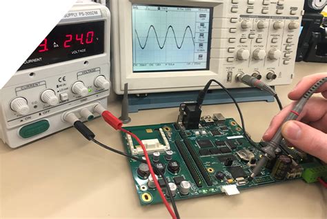
PCB Testing Equipment
To perform the various types of PCB tests, different equipment is used. Some of the common equipment includes:
-
Multimeters: Used for measuring voltage, current, and resistance.
-
Oscilloscopes: Used for visualizing and analyzing electrical signals.
-
Logic Analyzers: Used for capturing and analyzing digital signals.
-
In-Circuit Testers: Automated test equipment for performing ICT.
-
Flying Probe Testers: Automated test equipment for performing flying probe testing.
-
Boundary Scan Controllers: Used for performing boundary scan testing.
-
Functional Test Systems: Specialized equipment for performing functional testing.

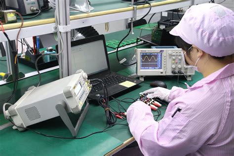
PCB Testing Processes
The PCB testing process typically involves the following steps:
-
Test Planning: Defining the test requirements, selecting the appropriate test methods, and creating test plans.
-
Test Fixture Design: Designing and fabricating test fixtures for ICT or other tests that require physical contact with the PCB.
-
Test Program Development: Creating test programs and scripts for automated testing.
-
Test Execution: Running the tests and collecting the results.
-
Result Analysis: Analyzing the test results to identify defects and issues.
-
Debugging and Repair: Debugging and repairing the PCBs based on the test results.
-
Reporting: Generating test reports and documentation for traceability and compliance purposes.
Best Practices for PCB Testing
To ensure effective and efficient PCB testing, consider the following best practices:
-
Design for Testability: Incorporate testability features into the PCB design, such as test points, boundary scan components, and clear labeling.
-
Choose the Right Tests: Select the appropriate test methods based on the complexity of the PCB, the production volume, and the specific requirements.
-
Develop Comprehensive Test Plans: Create detailed test plans that cover all the necessary tests and define the acceptance criteria.
-
Use Automated Testing: Implement automated testing wherever possible to reduce human error and increase efficiency.
-
Maintain Accurate Documentation: Keep accurate records of test results, defects, and repairs for traceability and continuous improvement.
Frequently Asked Questions (FAQ)
- What is the difference between ICT and flying probe testing?
-
ICT uses a fixed bed-of-nails fixture to test individual components, while flying probe testing uses movable probes. ICT is faster but requires custom fixtures, while flying probe testing is more flexible but slower.
-
Can all components on a PCB be tested using boundary scan?
-
No, boundary scan testing is limited to digital components that have built-in boundary scan support. It cannot test analog components or components without boundary scan capabilities.
-
How long does PCB testing take?
-
The duration of PCB testing depends on the complexity of the board, the types of tests performed, and the number of boards being tested. It can range from a few minutes to several hours per board.
-
Is PCB testing required for all types of electronic products?
-
While PCB testing is highly recommended for all electronic products to ensure quality and reliability, the specific testing requirements may vary depending on the industry, application, and regulatory standards.
-
Can PCB testing be outsourced to third-party service providers?
- Yes, many companies offer PCB testing services. Outsourcing testing can be cost-effective, especially for companies that do not have in-house testing capabilities or require specialized testing equipment.
Conclusion
PCB testing is a vital aspect of the electronics manufacturing process. It helps ensure the quality, reliability, and compliance of PCBs before they are assembled into the final product. By understanding the different types of tests, the equipment used, and the best practices for testing, manufacturers can implement effective testing strategies to minimize defects, reduce costs, and improve customer satisfaction.
As technology advances and PCBs become more complex, the importance of thorough and efficient testing will only continue to grow. Investing in the right testing equipment, processes, and expertise will be essential for companies to stay competitive and deliver high-quality electronic products to their customers.
No responses yet