What is SPI and Why is Trace Impedance Important?
Serial Peripheral Interface (SPI) is a synchronous serial communication interface used for short-distance communication between integrated circuits. It is widely used in embedded systems to connect microcontrollers to peripheral devices such as sensors, displays, and memory chips.
In an SPI system, trace impedance plays a crucial role in ensuring reliable communication and signal integrity. Trace impedance refers to the characteristic impedance of the conductive traces on a printed circuit board (PCB) that carry the SPI signals. Mismatched impedances can lead to signal reflections, distortions, and reduced signal quality, ultimately impacting the performance and reliability of the SPI communication.
Key Characteristics of SPI
- Full-duplex, synchronous serial communication protocol
- Master-slave architecture with a single master and one or more slaves
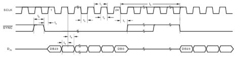
- Uses four signals: SCLK (serial clock), MOSI (master out, slave in), MISO (master in, slave out), and SS (slave select)
- Supports high-speed data transfer, typically up to tens of MHz
- Widely used in embedded systems and communication between ICs
Factors Affecting SPI Trace Impedance
Several factors influence the impedance of SPI traces on a PCB. Understanding these factors is essential for designing a robust SPI system with optimal signal integrity.
PCB Material and Thickness
The choice of PCB material and its thickness have a significant impact on trace impedance. The dielectric constant (Dk) and dissipation factor (Df) of the PCB material determine the capacitance and losses of the traces. Common PCB materials include FR-4, Rogers, and Isola, each with different electrical properties.
| Material | Dielectric Constant (Dk) | Dissipation Factor (Df) |
|---|---|---|
| FR-4 | 4.2 – 4.6 | 0.02 – 0.03 |
| Rogers | 2.2 – 10.2 | 0.0009 – 0.0035 |
| Isola | 3.0 – 4.0 | 0.002 – 0.02 |
The thickness of the PCB also affects trace impedance. Thicker PCBs generally have lower trace impedance due to increased capacitance between the trace and the ground plane.
Trace Width and Spacing
The width of the SPI traces and the spacing between them significantly influence the trace impedance. Wider traces have lower impedance, while narrower traces have higher impedance. The spacing between traces affects the coupling capacitance and crosstalk between adjacent traces.
To achieve a target impedance, designers can use PCB design tools and calculators to determine the appropriate trace width and spacing based on the PCB material and thickness.
Trace Length and Routing
The length of SPI traces and their routing on the PCB also impact trace impedance. Longer traces have higher impedance due to increased inductance and resistance. It is important to keep SPI traces as short as possible to minimize impedance mismatches and signal degradation.
Proper routing techniques, such as using continuous ground planes, avoiding sharp bends, and maintaining consistent trace widths, help maintain a consistent impedance along the trace length.
Calculating SPI Trace Impedance
To ensure optimal SPI performance, designers need to calculate and control the trace impedance. There are several methods and tools available for calculating SPI trace impedance.
Impedance Calculation Formulas
One approach to calculating trace impedance is using mathematical formulas based on the PCB geometry and material properties. The most common formula for microstrip traces (traces on the outer layer of the PCB) is:
Z0 = 87 / √(ɛr + 1.41) * ln(5.98 * h / (0.8 * w + t))
Where:
– Z0 is the characteristic impedance in ohms
– ɛr is the dielectric constant of the PCB material
– h is the height of the substrate (PCB thickness) in mils
– w is the width of the trace in mils
– t is the thickness of the trace in mils
For stripline traces (traces embedded within the PCB layers), the formula is slightly different:
Z0 = 60 / √ɛr * ln(4 * h / (0.67 * π * (0.8 * w + t)))
These formulas provide a rough estimate of the trace impedance but may not account for all the factors affecting the actual impedance.
PCB Design Tools and Calculators
Many PCB design software packages include built-in tools and calculators for determining trace impedance based on the PCB stackup, material properties, and trace geometry. These tools often provide more accurate results than manual calculations, as they consider a wider range of factors and use complex electromagnetic simulations.
Some popular PCB design tools with impedance calculators include:
- Altium Designer
- Cadence Allegro
- Mentor Graphics PADS
- KiCad
Online impedance calculators are also available, such as the Saturn PCB Toolkit and the EEWeb PCB Impedance Calculator, which allow designers to quickly estimate trace impedance based on basic parameters.

Impedance Matching Techniques
To ensure optimal signal integrity in SPI systems, designers need to match the impedance of the SPI traces to the impedance of the source and load devices. Several techniques can be used to achieve impedance matching.
Termination Resistors
One common method for impedance matching is using termination resistors at the end of the SPI traces. The termination resistor value should be equal to the characteristic impedance of the trace to minimize signal reflections.
There are three main types of termination:
- Series termination: A resistor is placed in series with the signal source, matching the source impedance to the trace impedance.
- Parallel termination: A resistor is placed in parallel with the signal load, matching the load impedance to the trace impedance.
- Thevenin termination: A combination of series and parallel resistors is used to match both the source and load impedances to the trace impedance.
The choice of termination technique depends on the specific requirements of the SPI system, such as the signal frequency, trace length, and driver characteristics.
Impedance-Controlled PCB Fabrication
For high-speed SPI systems, it is often necessary to use impedance-controlled PCB fabrication techniques to ensure consistent trace impedance across the board. This involves specifying the target impedance value to the PCB manufacturer, who will adjust the trace width, spacing, and dielectric thickness to achieve the desired impedance within a certain tolerance.
Impedance-controlled PCBs are more expensive than standard PCBs due to the additional manufacturing steps and testing required. However, they are essential for maintaining signal integrity in critical high-speed applications.
Differential Signaling
Another technique for improving SPI signal integrity is using differential signaling instead of single-ended signaling. In differential signaling, each SPI signal is transmitted using a pair of traces with opposite polarity. The receiver detects the difference between the two signals, which helps cancel out common-mode noise and interference.
Differential signaling requires a different approach to impedance matching, as the impedance of the differential trace pair must be matched to the differential impedance of the source and load devices. Differential impedance is typically specified as the odd-mode impedance, which is the impedance between the two traces when they carry equal and opposite currents.
Testing and Verification
After designing and fabricating an SPI system with controlled trace impedance, it is crucial to test and verify the actual impedance values to ensure they meet the target specifications. Several methods can be used for impedance testing.
Time Domain Reflectometry (TDR)
Time Domain Reflectometry (TDR) is a common technique for measuring trace impedance in the time domain. A TDR instrument sends a fast-rising pulse down the trace and measures the reflected signal. By analyzing the amplitude and timing of the reflections, the instrument can determine the impedance profile along the trace length.
TDR testing can identify impedance discontinuities, such as vias, connectors, and terminations, and help designers optimize the PCB layout for better signal integrity.
Vector Network Analyzer (VNA)
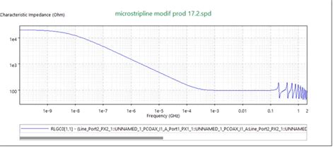
A Vector Network Analyzer (VNA) is another tool for measuring trace impedance, but in the frequency domain. A VNA measures the scattering parameters (S-parameters) of the trace, which characterize its impedance and transmission properties as a function of frequency.
VNA testing is particularly useful for high-frequency SPI systems, where the trace impedance may vary with frequency due to the skin effect and dielectric losses. By analyzing the S-parameters, designers can optimize the trace geometry and materials for the desired frequency range.
Impedance Test Coupons
Impedance test coupons are small PCB sections that are fabricated alongside the main PCB and contain representative traces with the same geometry and materials as the SPI traces. These coupons are used for destructive impedance testing, where the traces are probed or cut to measure their actual impedance.
Test coupons provide a cost-effective way to verify the impedance of the fabricated PCB without damaging the main board. They are especially useful for impedance-controlled PCBs, where the manufacturer can use the coupons to certify that the delivered boards meet the specified impedance tolerances.
Frequently Asked Questions (FAQ)
1. What is the typical impedance value for SPI traces?
The typical impedance value for SPI traces is 50 ohms, which matches the impedance of most SPI devices and test equipment. However, other impedance values, such as 75 ohms or 100 ohms, may be used depending on the specific application and system requirements.
2. Can I use the same impedance for all SPI signals?
Yes, it is generally recommended to use the same impedance for all SPI signals (SCLK, MOSI, MISO, and SS) to ensure consistent signal propagation and minimize reflections. However, in some cases, different impedance values may be used for certain signals, such as the slave select (SS) line, which is not part of the high-speed data transfer.
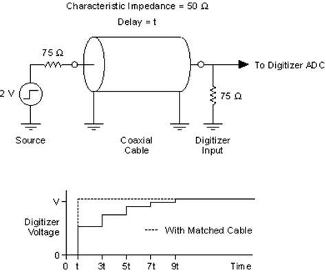
3. What happens if the SPI trace impedance is not matched?
If the SPI trace impedance is not matched to the impedance of the source and load devices, signal reflections can occur at the impedance discontinuities. These reflections can cause signal distortions, overshoot, undershoot, and ringing, which can lead to data corruption, reduced noise margin, and electromagnetic interference (EMI) issues.
4. How do I choose the right PCB material for SPI traces?
The choice of PCB material for SPI traces depends on several factors, including the desired impedance, signal frequency, dielectric constant, and dissipation factor. For high-speed SPI applications, low-loss materials with a stable dielectric constant, such as Rogers or Isola, are often preferred over standard FR-4. The PCB manufacturer can provide guidance on the most suitable material for a given application.
5. Can I use autorouting for SPI traces?
While autorouting can be used for SPI traces, it is generally not recommended for high-speed or impedance-controlled designs. Autorouting algorithms may not always generate the most optimal trace geometry and spacing for maintaining consistent impedance. It is better to manually route the SPI traces, following best practices for impedance control, such as using continuous ground planes, avoiding sharp bends, and minimizing trace length.
Conclusion
Designing SPI systems with proper trace impedance is essential for ensuring reliable communication and signal integrity. By understanding the factors affecting trace impedance, using appropriate calculation methods, and applying impedance matching techniques, designers can optimize their PCB layouts for optimal SPI performance.
Regular testing and verification of the fabricated PCBs are also crucial for validating the impedance control measures and identifying any issues early in the development process. By following best practices and working closely with PCB manufacturers, designers can create robust and high-quality SPI systems that meet the demanding requirements of modern electronic applications.
No responses yet