What is PCB Silk-Screening?
PCB silk-screening, also known as legend printing or nomenclature, is a process used to apply text, logos, and other markings onto the surface of a printed circuit board (PCB). This process involves using a fine mesh screen to transfer ink onto the PCB surface, creating a permanent and durable mark. Silk-screening is an essential part of the PCB manufacturing process, as it helps to identify components, provide assembly instructions, and improve the overall aesthetics of the board.
The Importance of PCB Silk-Screening
Silk-screening serves several important functions in the PCB manufacturing process:
-
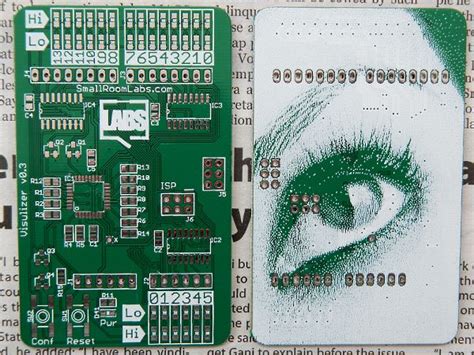
Component Identification: Silk-screening is used to label components on the PCB, such as resistors, capacitors, and integrated circuits. This helps technicians and engineers identify and troubleshoot components during assembly and maintenance.
-
Orientation Markings: Silk-screened markings can indicate the orientation of components, such as the polarity of capacitors or the pin numbering of integrated circuits. This ensures correct component placement during assembly.
-
Assembly Instructions: Silk-screening can provide assembly instructions, such as the order in which components should be placed or the location of test points. This can streamline the assembly process and reduce errors.
-
Branding and Aesthetics: Silk-screening can be used to apply company logos, product names, or other branding elements to the PCB. This can enhance the overall appearance of the product and reinforce brand identity.
The Silk-Screening Process
The PCB silk-screening process involves several steps:
-
Screen Preparation: A fine mesh screen is coated with a light-sensitive emulsion and exposed to UV light through a film positive of the desired artwork. The exposed areas of the emulsion harden, while the unexposed areas remain soluble.
-
Ink Preparation: The silk-screen ink is mixed and prepared according to the desired color and consistency. The ink must be compatible with the PCB surface material and able to withstand the soldering process.
-
Printing: The prepared screen is placed over the PCB, and ink is applied using a squeegee. The ink passes through the open areas of the screen and onto the PCB surface.
-
Curing: After printing, the ink is cured using heat or UV light to ensure a strong bond with the PCB surface. The curing process also ensures that the ink is resistant to solvents and abrasion.
Silk-Screening Materials
The materials used in PCB silk-screening must be carefully selected to ensure the best results:
-
Ink: PCB silk-screen inks are typically epoxy-based and formulated to withstand the high temperatures of the soldering process. They are available in various colors, including white, black, yellow, and red.
-
Screen: The screen used in silk-screening is typically made of a fine mesh polyester or stainless steel material. The mesh count, which refers to the number of openings per inch, determines the resolution and detail of the printed image.
-
Emulsion: The light-sensitive emulsion used to coat the screen is typically a diazo or photopolymer material. The emulsion must be compatible with the ink and able to produce a sharp, well-defined image.

Advantages of PCB Silk-Screening
PCB silk-screening offers several advantages over other marking methods, such as ink-jet printing or laser marking:
-
Durability: Silk-screened markings are highly durable and resistant to abrasion, solvents, and high temperatures. This ensures that the markings remain legible throughout the life of the PCB.
-
Precision: Silk-screening can produce high-resolution images with fine detail, making it suitable for small components and dense PCB layouts.
-
Versatility: Silk-screening can be used on a variety of PCB surface materials, including FR-4, aluminum, and flexible substrates.
-
Cost-effectiveness: Silk-screening is a cost-effective marking method, particularly for high-volume production runs. The screens can be reused multiple times, reducing the cost per unit.

Challenges in PCB Silk-Screening
Despite its many advantages, PCB silk-screening does present some challenges:
-
Design Limitations: The resolution of silk-screened images is limited by the mesh count of the screen. Fine details or small text may be difficult to reproduce accurately.
-
Registration: Ensuring precise alignment between the screen and the PCB can be challenging, particularly for double-sided or multi-layer boards.
-
Ink Compatibility: The silk-screen ink must be compatible with the PCB surface material and able to withstand the soldering process without smudging or fading.
-
Environmental Concerns: Some silk-screen inks contain volatile organic compounds (VOCs) or other hazardous substances that may require special handling and disposal.

Best Practices for PCB Silk-Screening
To ensure the best results from PCB silk-screening, consider the following best practices:
-
Design for Manufacturability: When designing the silk-screen artwork, consider the limitations of the printing process. Use clear, legible fonts and ensure that the artwork is compatible with the screen mesh count.
-
Use High-Quality Materials: Choose high-quality inks, screens, and emulsions to ensure the best print quality and durability.
-
Optimize the Printing Process: Ensure that the screen is properly tensioned and aligned with the PCB. Use the appropriate squeegee pressure and angle to achieve a consistent print.
-
Perform Quality Control: Inspect the printed PCBs for accuracy, legibility, and adherence to specifications. Use magnification or automated inspection systems to detect defects or inconsistencies.
The Future of PCB Silk-Screening
As PCB technology continues to evolve, so too does the silk-screening process. Some emerging trends and developments include:
-
Inkjet Printing: Inkjet printing is becoming an increasingly popular alternative to traditional silk-screening. This method offers higher resolution and greater design flexibility but may not be as durable or cost-effective for high-volume production.
-
Laser Marking: Laser marking uses a focused beam of light to etch markings directly onto the PCB surface. This method offers high precision and permanence but may be more expensive than silk-screening.
-
Conductive Inks: Researchers are developing conductive inks that can be used to print functional circuits directly onto the PCB surface. This could enable new design possibilities and streamline the manufacturing process.
-
Sustainable Materials: As environmental concerns grow, there is increasing interest in sustainable and eco-friendly silk-screening materials, such as water-based inks and biodegradable screens.
Frequently Asked Questions (FAQ)
-
What is the difference between silk-screening and other PCB marking methods?
Silk-screening is a printing method that uses a fine mesh screen to transfer ink onto the PCB surface. It offers high durability, precision, and cost-effectiveness compared to other methods like ink-jet printing or laser marking. -
Can silk-screening be used on any PCB surface material?
Silk-screening is versatile and can be used on a variety of PCB surface materials, including FR-4, aluminum, and flexible substrates. However, the ink and printing process may need to be optimized for each material. -
How long do silk-screened markings last?
Silk-screened markings are highly durable and can last throughout the life of the PCB. They are resistant to abrasion, solvents, and high temperatures, ensuring long-term legibility. -
What is the resolution limit of silk-screening?
The resolution of silk-screened images is limited by the mesh count of the screen. Higher mesh counts allow for finer details and smaller text, but there are practical limitations to the achievable resolution. -
Are there any environmental concerns with silk-screening?
Some silk-screen inks contain volatile organic compounds (VOCs) or other hazardous substances that may require special handling and disposal. However, there is growing interest in sustainable and eco-friendly silk-screening materials, such as water-based inks and biodegradable screens.
Conclusion
PCB silk-screening is a critical process in the manufacturing of printed circuit boards, providing essential component identification, assembly instructions, and branding elements. By understanding the silk-screening process, materials, and best practices, PCB Designers and manufacturers can ensure high-quality, durable, and legible markings on their boards. As PCB technology continues to advance, the silk-screening process will likely evolve to meet new challenges and opportunities, such as inkjet printing, laser marking, and sustainable materials. Ultimately, the goal of PCB silk-screening remains the same: to enhance the functionality, reliability, and aesthetics of printed circuit boards.

No responses yet